A cross-shaped photonic crystal waveguide formed by a square lattice rods array is numerically and experimentally investigated. The band gap of the TE mode for the photonic crystals and transmission characteristics of waveguides are calculated by the plane wave expansion method and the finite element method. We perform the experiments in the microwave regime to validate the numerical results. The measured reflection and transmission characteristics of the photonic crystals show a large band gap between 8.62 and 11.554 GHz (relative bandwidth is 29.34%). The electromagnetic waves are transmitted stably in the waveguides, and the transmission characteristics maintain a high level in the band gap.
In the recent years, photonic crystals (PCs) have attracted a lot of attention, since they can be used in the controlling of light flow based on the photonic band gap (PBG)[1]. By enhancing and manipulating the light trapping efficiency, these structures can contribute significant applications in linear and nonlinear photonic devices like isolators[2], solar cells[3], mirrors[4], waveguides[5], lasers and cavities[6,7], filters[8,9], circulators[10–13], and other important components for high density optical integration[14,15].
Although the PC waveguides (PCWs) have received significant attention[16–21], their transmission and especially the PCW with a wide bandwidth have been much less studied. Based on the characteristics of the PBG, designing PCW with a larger PBG will produce significant impacts both in academic and application areas.
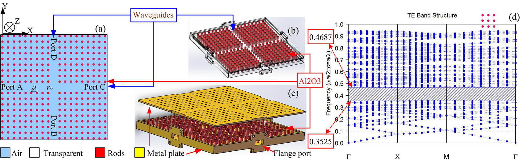
In this study, we focus on developing a new two-dimensional (2D) square lattice PC structure with a larger PBG, which can be used to design a cross-shaped PCW with a wide bandwidth, as shown in Fig. 1. The basic ingredient of the PCW structure in our case is a square lattice rods array, distributing in the air with two rows of line defects, whose structural parameters are presented in Fig. 1(a). The radius of the rods is with . The lattice constant is represented by .
Sign up for Chinese Optics Letters TOC. Get the latest issue of Chinese Optics Letters delivered right to you!Sign up now
Figure 1.(a) 2D PCs defect structure; (b) 2D square lattice PCW in a transparent shell; (c) schematic diagram of the PCW; (d) PBG of the 2D square lattice PCs.
The PBGs are calculated by using commercially available photonic band calculation software (BandSOLVE, Rsoft Design Group), and the numerical analysis here is only carried out for TE polarization, as shown in Fig. 1(d). A wide PBG is obtained by the plane wave expansion method, which is expressed as the normalized frequency range of , and the central frequency is , where is the speed of the light. In principle, the PC structure forbids the propagation of electromagnetic waves within this PBG frequency range and reflects impinging light waves back.
The schematic diagram of the PCW is envisaged by inserting a 2D square lattice dielectric rods array (red) in a rectangular metal waveguide with a transparent shell, as shown in Fig. 1(b). In order to guarantee the PBG characteristic of PC, it is necessary to ensure the high precision of the periodic structure. Here, a metal waveguide (yellow) is used to fix the dielectric rods, and in this way, precision machining can be obtained, as shown in Fig. 1(c). Four flange interfaces are designed to be used in connection with the test equipment.
As shown in Fig. 2, the function of the PCW and the electromagnetic field propagation are simulated by the finite element method. The calculated region is divided into about 100,000 grid cells, and the boundary condition is set for the scattering boundary condition. The numerical results show that the electromagnetic waves launched from Port A are transmitted stably to Ports B, C, and D in the waveguides at the central frequency of , as shown in Fig. 2(a). The amplitude of the output port is almost same with the input port, as shown in Fig. 2(b). The power of the electromagnetic waves divided into three parts are transmitted into the three output ports, and the output power of Port C is slightly larger than the power of Port B or D, as shown in Figs. 2(e) and 2(f). The transmission efficiencies of the Ports B, C, and D to Port A, respectively, are 24.8%, 25.3%, and 24.8%, and total transmission efficiency of the PCW is 74.9%. However, there is no optical local effect of the PCW. The energy spread in the PCs at the normalized frequency of and away from the frequency range of the PBG are shown in Figs. 2(c), 2(d), 2(g), and 2(h), respectively.
Figure 2.(a) Ez field distribution in the PCW; (b) the amplitude of the Ez field; (c) and (d) the distribution of power in the PCs at the normalized frequency of ; (e) and (f) the distribution of power in the PCW at the central frequency of ; (g) and (h) the distribution of power in the PCs at the central frequency of .
In order to validate the aforementioned numerical results, the experiments are carried out in the microwave regime using an Agilent E8361C vector network analyzer. The PCs structure sample is formed by inserting a 2D square lattice ceramic rods array (with the lattice constant ) in a rectangular aluminous waveguide (). The size of the flange port is . Cylindrical 99% dielectric rods with a radius of (about 2 mm) were used in the experiments, and its permittivity is 9.2. The sectional view of the PCs sample with the foam plastic double-layer flat plate absorbing material (black) at each side of the rods array is shown in Fig. 3(a). The frequency range of the electromagnetic waves that can be absorbed in the material is 4–18 GHz.
Figure 3.(a) Sectional view of the PCs sample; (b) experimental setup for measuring the PBG of the PCs.
The experiment set for measuring transmission through the PCs is shown in Fig. 3(b). The PCs sample and the vector network analyzer are connected through the SubMiniature version A (SMA) connector and waveguide to the coaxial converter. In the scanning frequency range of 7 to 13 GHz, the reflection and transmission characteristics of the PCs are measured, as shown in Fig. 4. Since the numerical central frequency is 10.04 GHz, which is calculated by , in the experiment, the central frequency is chosen to be 10 GHz.
Figure 4.(a) Logarithmic value of the reflection efficiency of Port A; (b) the isolation of Ports B to A; (c) the isolation of Ports A to B; (d) the logarithmic value of the reflection efficiency of Port B.
In the experiments, parameter represents the logarithmic value of the ratio of the reflected power to the input power of Port 1. Parameter represents the logarithmic value of the ratio of the output power of Port 2 from the input power of Port 1. Similarly, and represent the reflection and transmission characteristics of Port 2. In the classical measurement of the network analyzer, the S parameters are, respectively, expressed as follows: where and are the input power of Ports 1 and 2. and are the reflected power of Ports 1 and 2. is the transmission power from Port 1 to Port 2, and is the transmission power from Port 2 to Port 1.
In Figs. 4(b) and 4(c), it is obvious that the transmission efficiencies between Port 1 and Port 2 are (Ports 1 to 2) and (Ports 2 to 1) at the central frequency of 10 GHz. That means that there is almost no energy from one port transmitting to another. The reason is that the PC plays a role in the isolation.
When the insertion loss of the electric cable and adapter is ignored, reflection coefficients and isolation of the PCs are, respectively, expressed as follows: where and are the reflection efficiencies of the PCs, and and are the isolation of Port B to Port A or Port A to Port B. As shown in Figs. 4(b) and 4(c), the experimental results show that there is an ultra-wide PBG of 8.62–11.554 GHz (). Reflection coefficients and in Figs. 4(a) and 4(d) change smoothly in the frequency range of the PBG, and the reflection coefficients are approximately (about 90.2%) at the central frequency of 10 GHz. That means that more than 90% energy is reflected back to the input port by the PCs with a low loss.
Furthermore, the experimental setup for validating the transmission characteristics of the cross-shaped PCW is shown in Fig. 5. The ceramic rods array with two rows of line defects are fixed by the upper and bottom plate of the brass waveguide, as shown in Fig. 5(a). The transmission efficiency is tested by connecting the load to the other two ports shown in Figs. 5(b) and 5(c), which can be expressed as follows: where and are the output power of Port C and Port D from input Port A, and and are the transmission efficiencies of Port C to Port A or Port D to Port A, whose logarithmic value is represent by the parameter in Fig. 6.
Figure 5.(a) Sectional view of the PCW sample; (b) experimental setup for measuring the transmission efficiency between Port A and Port C; (c) experimental setup for measuring the transmission efficiency between Port A and Port D.
Figure 6.Logarithmic value of the transmission efficiency between Port A and Port C: (a) and (b) ; Logarithmic value of the transmission efficiency between Port A and Port D: (c) and (d) .
The experimental results show that there is stable transmission in the PCW. The transmission efficiencies change smoothly in the aforementioned PBG of 8.62–11.554 GHz, as shown in Fig. 6. The transmission efficiency inside the PBG is smooth, while it still fluctuated when outside the PBG. The transmission efficiencies of some frequencies outside the PBG are as high as the transmission inside the PBG. At the central frequency of 10 GHz, transmission efficiency of (26.4%) is higher than of (23.1%), as shown in Figs. 6(a) and 6(c), respectively. The transmission efficiency of Ports C to A or Ports D to A represented by parameter has the same changing trend with parameter , as shown in Figs. 6(b) and 6(d). Due to the symmetrical structure of the PCW, the transmission efficiency of Ports A to B is considered to be the same as Ports A to D, and the total transmission efficiency of the PCW is 72.6%, which is perfectly consistent with the numerical value. The transmission performance of the PCW deteriorates significantly beyond the range of the PBG.
A comparison is made between the experimental and numerical results, as shown in Table 1. It is obvious that there is a perfect agreement on the central frequency between the experimental and numerical results. The PBG of the PCs has a slightly red shift, and the possible reason is that the actual dielectric constant of the rods is slightly larger than 9.2. But, it is surely because the width (about 29%) of the PBG is strikingly consistent between the experimental and numerical results. The isolation of the PCs is up to , and reflection efficiencies of the PCs are higher than 90% at the central frequency. The reflection efficiencies of the PCs in Figs. 4(a) and 4(d) maintain a high level in a relatively large frequency range. Furthermore, the transmission efficiency of the PCW maintains a stable level in the frequency range in Figs. 6 and reaches 72.9% at the central frequency, which is consistent with the numerical value of 74.9%.
Numerical value
Normalized frequency range of PBG
0.3525(2πc/a)–0.4687(2πc/a)
Normalized central frequency
0.4016(2πc/a)
Frequency range of PBG
8.81–11.72 GHz (29.1%)
Central frequency f0
10.04 GHz
Transmission efficiency at f0
74.9%
Experimental value
f0
10 GHz
τBA at f0
−55.67dB
τAB at f0
−57.24dB
Frequency range of PBG (τ<−20dB)
8.62–11.554 GHz (relative bandwidth is 29.34%)
RA at f0
−0.45dB (90.2%)
RB at f0
−0.45dB (90.2%)
Transmission efficiency at f0
72.9%
Table 1. Comparison Between Experimental and Numerical Results
In conclusion, a newly cross-shaped PCW with the ultra-wide PBG (relative bandwidth is 29.34%) formed by the 99% rods array is numerically and experimentally investigated. At the central frequency, the isolation of PCs reaches , and the transmission efficiency of the PCW is approximately 73%. As to the PCW, it should be noted that the process is relatively simple, and the material can be obtained easily. The excellent performance of the PBG and low material loss demonstrate that square lattice PCs using 99% rods is a promising method for generating an optical waveguide or other optical devices with a large PBG in integrated optical communication in the future. If some non-reciprocal sample, such as a ferrite post biased external magnet is put in the central point of the waveguide junction, a circulator with a 2D PCs structure may be realized in the frequency of the PBG of PCs.