• Chinese Journal of Lasers
  • Vol. 47, Issue 1, 0100002 (2020)
Xiaofeng Liu1、2、3, Liping Peng2、3、4, Yuanan Zhao2、3、5、*, Xi Wang1, Dawei Li2、3, and Jianda Shao2、3、**
Author Affiliations
  • 1State Key Laboratory of Pulsed Power Laser Technology, National University of Defense Technology,Hefei, Anhui 230037, China
  • 2Laboratory of Thin Film Optics, Shanghai Institute of Optics and Fine Mechanics, Chinese Academy of Sciences,Shanghai 201800, China
  • 3Key Laboratory of Materials for High Power Laser, Chinese Academy of Sciences, Shanghai 201800, China
  • 4Center of Materials Science and Optoelectronics Engineering, University of Chinese Academy of Sciences,Beijing 100049, China
  • 5State Key Laboratory of Applied Optics, Changchun Institute of Optics, Fine Mechanics and Physics,Chinese Academy of Sciences, Changchun, Jilin 130033, China
  • show less
    DOI: 10.3788/CJL202047.0100002 Cite this Article Set citation alerts
    Xiaofeng Liu, Liping Peng, Yuanan Zhao, Xi Wang, Dawei Li, Jianda Shao. Research Progress on Near-Infrared High-Power Laser Damage of Liquid Crystal Optical Devices[J]. Chinese Journal of Lasers, 2020, 47(1): 0100002 Copy Citation Text show less
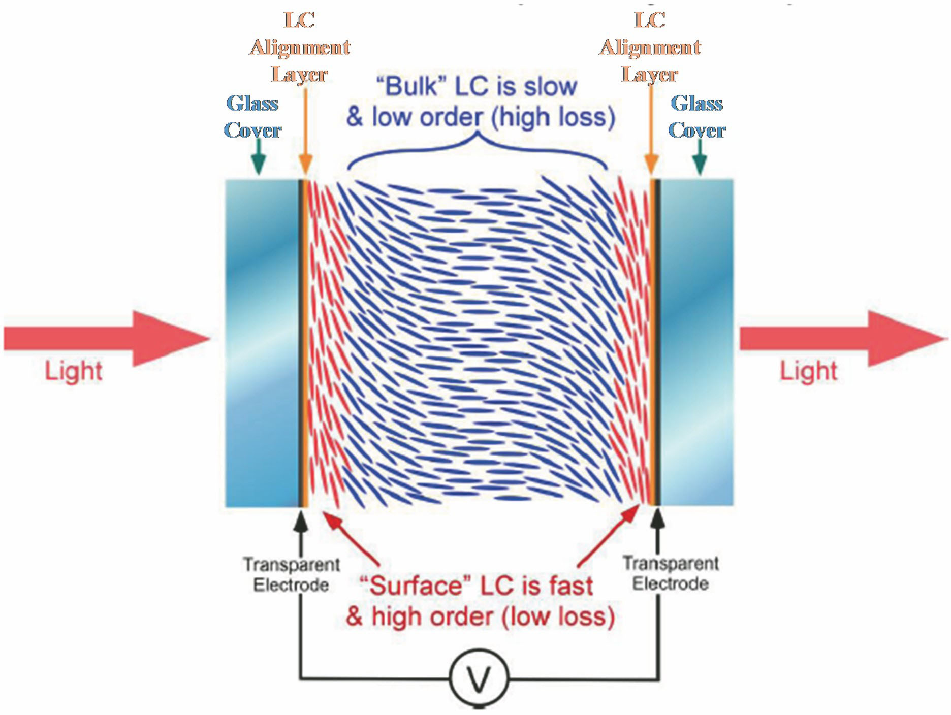
    Basic structure of liquid crystal optical device[20]
    Fig. 1. Basic structure of liquid crystal optical device[20]
    Diagrams of liquid crystal molecule rotation[21].(a) No voltage is applied; (b) voltage is applied
    Fig. 2. Diagrams of liquid crystal molecule rotation[21].(a) No voltage is applied; (b) voltage is applied
    Laser induced damage thresholds of ITO films with different thicknesses[29]. (a) 300 nm; (b) 100 nm; (c) 50 nm
    Fig. 3. Laser induced damage thresholds of ITO films with different thicknesses[29]. (a) 300 nm; (b) 100 nm; (c) 50 nm
    Microstructures and spectra of ITO films with different thicknesses[29]. (a) Microstructures; (b) spectra
    Fig. 4. Microstructures and spectra of ITO films with different thicknesses[29]. (a) Microstructures; (b) spectra
    Degeneration of surface state of 90-nm ITO film observed by optical microscope with laser irradiation energy and damage size[32]
    Fig. 5. Degeneration of surface state of 90-nm ITO film observed by optical microscope with laser irradiation energy and damage size[32]
    Damage of ITO film in Fig. 5 induced by energy density of 4.5 J/cm2 observed by scanning electron microscope (the scale bar is 400 nm)[32]
    Fig. 6. Damage of ITO film in Fig. 5 induced by energy density of 4.5 J/cm2 observed by scanning electron microscope (the scale bar is 400 nm)[32]
    Laser induced damage thresholds of ITO films (with thickness in the range from 10 nm to 100 nm) irradiated by pulses with different pulse durations (threshold temperature represented by the solid line is 1800 K, and threshold temperature represented by the dotted line is 1000 K)[34]
    Fig. 7. Laser induced damage thresholds of ITO films (with thickness in the range from 10 nm to 100 nm) irradiated by pulses with different pulse durations (threshold temperature represented by the solid line is 1800 K, and threshold temperature represented by the dotted line is 1000 K)[34]
    Typical damage morphologies of PI film under different laser irradiation. (a)-(c) Ultraviolet ps laser with wavelength of 355 nm; (d)-(f) near-infrared ps laser with wavelength of 1064 nm[44]
    Fig. 8. Typical damage morphologies of PI film under different laser irradiation. (a)-(c) Ultraviolet ps laser with wavelength of 355 nm; (d)-(f) near-infrared ps laser with wavelength of 1064 nm[44]
    Typical damage morphologies of PI film irradiated by the quasi-continuous nanosecond laser with the repetition rate of 20 kHz[45]. (a) Result observed by the white light interferometer (the parameter of the irradiated laser: 20.7 J/cm2, 50 pluses); (b) result observed by the microscopy (the parameter of the irradiated laser: 23 J/cm2, 500 pluses); (c) result observed by the SEM (the parameter of the irradiated laser: 19 J/cm
    Fig. 9. Typical damage morphologies of PI film irradiated by the quasi-continuous nanosecond laser with the repetition rate of 20 kHz[45]. (a) Result observed by the white light interferometer (the parameter of the irradiated laser: 20.7 J/cm2, 50 pluses); (b) result observed by the microscopy (the parameter of the irradiated laser: 23 J/cm2, 500 pluses); (c) result observed by the SEM (the parameter of the irradiated laser: 19 J/cm
    Judgment of laser damage of liquid crystal material using image subtraction[57]. (a) Image before laser irradiation; (b) image after laser irradiation; (c) result that the image before laser irradiation is subtracted from the image after laser irradiation
    Fig. 10. Judgment of laser damage of liquid crystal material using image subtraction[57]. (a) Image before laser irradiation; (b) image after laser irradiation; (c) result that the image before laser irradiation is subtracted from the image after laser irradiation
    Migration of the liquid crystal material under different control modes[28]. (a) Under irradiation of high power continuous laser; (b) under heating of temperature controller
    Fig. 11. Migration of the liquid crystal material under different control modes[28]. (a) Under irradiation of high power continuous laser; (b) under heating of temperature controller
    Thickness /nmCarrier density /cm-3Carrier mobility /(cm2·V-1·s-1)
    3005.0×102023.21
    1003.2×102022.98
    501.2×102022.00
    Table 1. Carrier density and carrier mobility of ITO films with different thicknesses[29]
    Liquid crystalmodulator elementLaser damage resistancewhen wavelength is 1064 nmand impulse durationis 15 ns /(J·cm-2)
    Glass substrate (K8)>16.0
    Liquid crystal layer>16.0
    Alignment layer (GeO)6.9
    ITO transparent electrode2.5-2.9
    Liquid crystal modulator withlongitudinal electric field2.5-2.9
    Table 2. Laser induced damage thresholds of liquid crystal optical devices and its components[25]
    Xiaofeng Liu, Liping Peng, Yuanan Zhao, Xi Wang, Dawei Li, Jianda Shao. Research Progress on Near-Infrared High-Power Laser Damage of Liquid Crystal Optical Devices[J]. Chinese Journal of Lasers, 2020, 47(1): 0100002
    Download Citation