• Chinese Journal of Lasers
  • Vol. 50, Issue 1, 0113010 (2023)
Yuanfei Hu1, Junrong Zheng1, Enming You1、**, and Songyuan Ding2、*
Author Affiliations
  • 1College of Chemistry and Chemical Engineering, Xiamen University, Xiamen 361005, Fujian, China
  • 2School of Physics and Optoelectronic Engineering, Hangzhou Institute for Advanced Study, University of Chinese Academy of Sciences, Hangzhou 310024, Zhejiang, China
  • show less
    DOI: 10.3788/CJL221180 Cite this Article Set citation alerts
    Yuanfei Hu, Junrong Zheng, Enming You, Songyuan Ding. Sub‑10 nm Ultrathin Metal Films: Preparation, Optical Properties, and Applications[J]. Chinese Journal of Lasers, 2023, 50(1): 0113010 Copy Citation Text show less
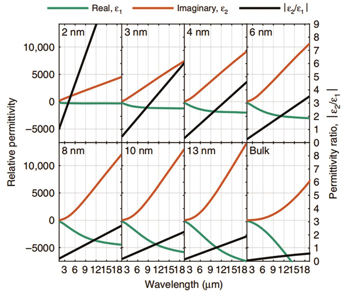
    Relative permittivities of ultrathin gold films with different thicknesses[14]
    Fig. 1. Relative permittivities of ultrathin gold films with different thicknesses[14]
    Wettability of metal on substrate surface is described by Young's equation[21]
    Fig. 2. Wettability of metal on substrate surface is described by Young's equation[21]
    Surface morphologies of 6-nm-thick silver films prepared with different seed layers[18]. (a) No seed layer; (b) seed layer is 1-nm-thick Cu; (c) seed layer is 1-nm-thick Si; (d) seed layer is 1-nm-thick Ti
    Fig. 3. Surface morphologies of 6-nm-thick silver films prepared with different seed layers[18]. (a) No seed layer; (b) seed layer is 1-nm-thick Cu; (c) seed layer is 1-nm-thick Si; (d) seed layer is 1-nm-thick Ti
    Characterization results of thickness and morphology of 3 nm ultrathin gold films[30]. (a) Height profile and (b) STEM image for 3-nm-thick gold film grown on 1-nm-thick copper seed layer; SEM images of (c) 3-nm-thick gold film without seed layer and (d) 3-nm-thick gold film with seed layer
    Fig. 4. Characterization results of thickness and morphology of 3 nm ultrathin gold films[30]. (a) Height profile and (b) STEM image for 3-nm-thick gold film grown on 1-nm-thick copper seed layer; SEM images of (c) 3-nm-thick gold film without seed layer and (d) 3-nm-thick gold film with seed layer
    Principle of organic modification method and surface morphologies of prepared ultrathin gold film[12,41-42]. (a) Principle of preparing ultrathin gold films by MPTMS; (b)principle of preparing ultrathin gold film by APTMS ; (c) SEM image of surface morphology of ultrathin gold film without adhesion layer ; (d) SEM image of surface morphology of ultrathin gold film prepared by MPTMS adhesion layer; (e) SEM image of surface morphology of ultrathin gold film prepared by APTMS adhesion layer
    Fig. 5. Principle of organic modification method and surface morphologies of prepared ultrathin gold film[12,41-42]. (a) Principle of preparing ultrathin gold films by MPTMS; (b)principle of preparing ultrathin gold film by APTMS ; (c) SEM image of surface morphology of ultrathin gold film without adhesion layer ; (d) SEM image of surface morphology of ultrathin gold film prepared by MPTMS adhesion layer; (e) SEM image of surface morphology of ultrathin gold film prepared by APTMS adhesion layer
    Diagram of co-deposition and SEM images and surface morphologies of silver films[19]. (a) Diagram of co-deposition; (b) SEM image of 9 nm pure Ag film with surface morphology shown in inset; (c) SEM image of 9 nm Al-doped Ag film with surface morphology shown in inset
    Fig. 6. Diagram of co-deposition and SEM images and surface morphologies of silver films[19]. (a) Diagram of co-deposition; (b) SEM image of 9 nm pure Ag film with surface morphology shown in inset; (c) SEM image of 9 nm Al-doped Ag film with surface morphology shown in inset
    Results of low temperature deposition[20]. (a) Diagram of low temperature deposition; (b)-(e) SEM images of 5-nm-thick gold films deposited at different temperatures; (f) block resistance of ultra-thin gold films as a function of deposition temperature
    Fig. 7. Results of low temperature deposition[20]. (a) Diagram of low temperature deposition; (b)-(e) SEM images of 5-nm-thick gold films deposited at different temperatures; (f) block resistance of ultra-thin gold films as a function of deposition temperature
    SEM and TEM images of 8-nm-thick gold nanoshells[64]. (a) SEM image; (b) TEM image
    Fig. 8. SEM and TEM images of 8-nm-thick gold nanoshells[64]. (a) SEM image; (b) TEM image
    Red-shifting of plasmon of UTMF. (a) Dipole resonance frequencies of 1-5 layer metal disks as a function of diameter [72]; (b) schematic and SEM images of ultrathin Ag film ribbon [73]; (c) dispersion curves of Au film ribbons with different thicknesses[30];(d) normalized extinction spectra of Ag film ribbons with width of 70 nm and different film thicknesses[73]; (e) extinction spectra of SiO2 nanoparticles containing 8-32 nm thick gold shells[62]
    Fig. 9. Red-shifting of plasmon of UTMF. (a) Dipole resonance frequencies of 1-5 layer metal disks as a function of diameter [72]; (b) schematic and SEM images of ultrathin Ag film ribbon [73]; (c) dispersion curves of Au film ribbons with different thicknesses[30];(d) normalized extinction spectra of Ag film ribbons with width of 70 nm and different film thicknesses[73]; (e) extinction spectra of SiO2 nanoparticles containing 8-32 nm thick gold shells[62]
    Gate-tunable plasmons in UTMF. (a) Extinction spectra of single-atom layer gold disk and gold sphere with diameter of 20 nm as a function of doping charge density[8] ; (b) ratio of resonance energy offset to full width at half-maximum as a function of doping concentration for gold disk and gold sphere[8]; (c) measured offsets of plasmonic resonant wavelength in whole voltage cycle for UTMF with different thicknesses [30]; (d) simulated shift of plasmonic resonant wavelength by varying effective surface carrier density with conceptual view of dynamic tuning of UTMF nanoribbons by ion-gel gating shown in inset[30]
    Fig. 10. Gate-tunable plasmons in UTMF. (a) Extinction spectra of single-atom layer gold disk and gold sphere with diameter of 20 nm as a function of doping charge density[8] ; (b) ratio of resonance energy offset to full width at half-maximum as a function of doping concentration for gold disk and gold sphere[8]; (c) measured offsets of plasmonic resonant wavelength in whole voltage cycle for UTMF with different thicknesses [30]; (d) simulated shift of plasmonic resonant wavelength by varying effective surface carrier density with conceptual view of dynamic tuning of UTMF nanoribbons by ion-gel gating shown in inset[30]
    Electrical and optical properties of ultrathin gold films[15]. (a) Schematics of prepared structure and incident direction of detection light; (b) resistivity and sheet resistance of Au films as a function of deposited thickness; (c) transmission and reflection spectra of Au films with different thicknesses; (d) experimental (left) and simulated (right) absorption spectra of ultrathin gold films with different thicknesses
    Fig. 11. Electrical and optical properties of ultrathin gold films[15]. (a) Schematics of prepared structure and incident direction of detection light; (b) resistivity and sheet resistance of Au films as a function of deposited thickness; (c) transmission and reflection spectra of Au films with different thicknesses; (d) experimental (left) and simulated (right) absorption spectra of ultrathin gold films with different thicknesses
    Nonlinear response of ultrathin metal films. (a) AFM images of prepared gold films with different thicknesses[81] ; (b) measured third-order polarizability of gold films[81]; (c) STEM image of metal quantum well cross section[82] ; (d) closed-loop z-scan curves for gold films with thicknesses of 3 nm and 15 nm[82]; (e) variation of calculated second harmonic, third harmonic and Kerr nonlinear polarizability with thickness and wave vector[9]
    Fig. 12. Nonlinear response of ultrathin metal films. (a) AFM images of prepared gold films with different thicknesses[81] ; (b) measured third-order polarizability of gold films[81]; (c) STEM image of metal quantum well cross section[82] ; (d) closed-loop z-scan curves for gold films with thicknesses of 3 nm and 15 nm[82]; (e) variation of calculated second harmonic, third harmonic and Kerr nonlinear polarizability with thickness and wave vector[9]
    Properties of transparent electrode. (a) Schematic of flexible polymer light-emitting diodes (PLEDs) using ultrathin Ni-doped Ag-based flexible transparent electrode[86] ; (b) external quantum efficiencies of Ni-doped Ag-based and ITO-based PLEDs[86]; (c) calculated and measured transmittance curves of transparent electrode with dielectric-metal-dielectric structure[87]; (d) photograph of fabricated flexible electrode[87]
    Fig. 13. Properties of transparent electrode. (a) Schematic of flexible polymer light-emitting diodes (PLEDs) using ultrathin Ni-doped Ag-based flexible transparent electrode[86] ; (b) external quantum efficiencies of Ni-doped Ag-based and ITO-based PLEDs[86]; (c) calculated and measured transmittance curves of transparent electrode with dielectric-metal-dielectric structure[87]; (d) photograph of fabricated flexible electrode[87]
    Development history of ultrathin metal film
    Fig. 14. Development history of ultrathin metal film
    MethodSubstrateThickness and materialAdhesion layerPercolation threshold /nmRq /nmRef.
    Seed layerGlass9 nm AgNi-Cr-2.211
    Fused silica6 nm AgCu30.418
    CaF23 nm AuCu(Cu2O)10.2230
    SixNy/Si2 nm AuCu(Cu2O)1.840.01914
    CaF2

    4 nm Au

    4 nm Ag

    CuO1.2

    0.21

    0.27

    31
    Organic modificationSi8 nm AuMPTMS-0.712
    Si6 nm AuAPTMS50.341
    SiO2/Si8 nm AuAPTMS-0.340
    Co-depositionSiO2/Si6 nm Al-doped Ag--0.3744
    Flexible transparent conductor7 nm Ni-doped Ag--0.5745
    Glass4 nm Al-doped AgTa2O540.7665
    Cryogenic depositionFused silica4 nm Au-30.2420
    ALDSi20-30 nm Au--6-959
    Chemical synthesisSiO28 nm Au---64
    Table 1. Summary of relevant work for each method
    Yuanfei Hu, Junrong Zheng, Enming You, Songyuan Ding. Sub‑10 nm Ultrathin Metal Films: Preparation, Optical Properties, and Applications[J]. Chinese Journal of Lasers, 2023, 50(1): 0113010
    Download Citation