
Tianbao Liu, Meiping Zhu, Wenyun Du, Jun Shi, Jian Sun, Yingjie Chai, Jianda Shao, "A nodule dome removal strategy to improve the laser-induced damage threshold of coatings," High Power Laser Sci. Eng. 10, 05000e30 (2022)
- High Power Laser Science and Engineering
- Vol. 10, Issue 5, 05000e30 (2022)
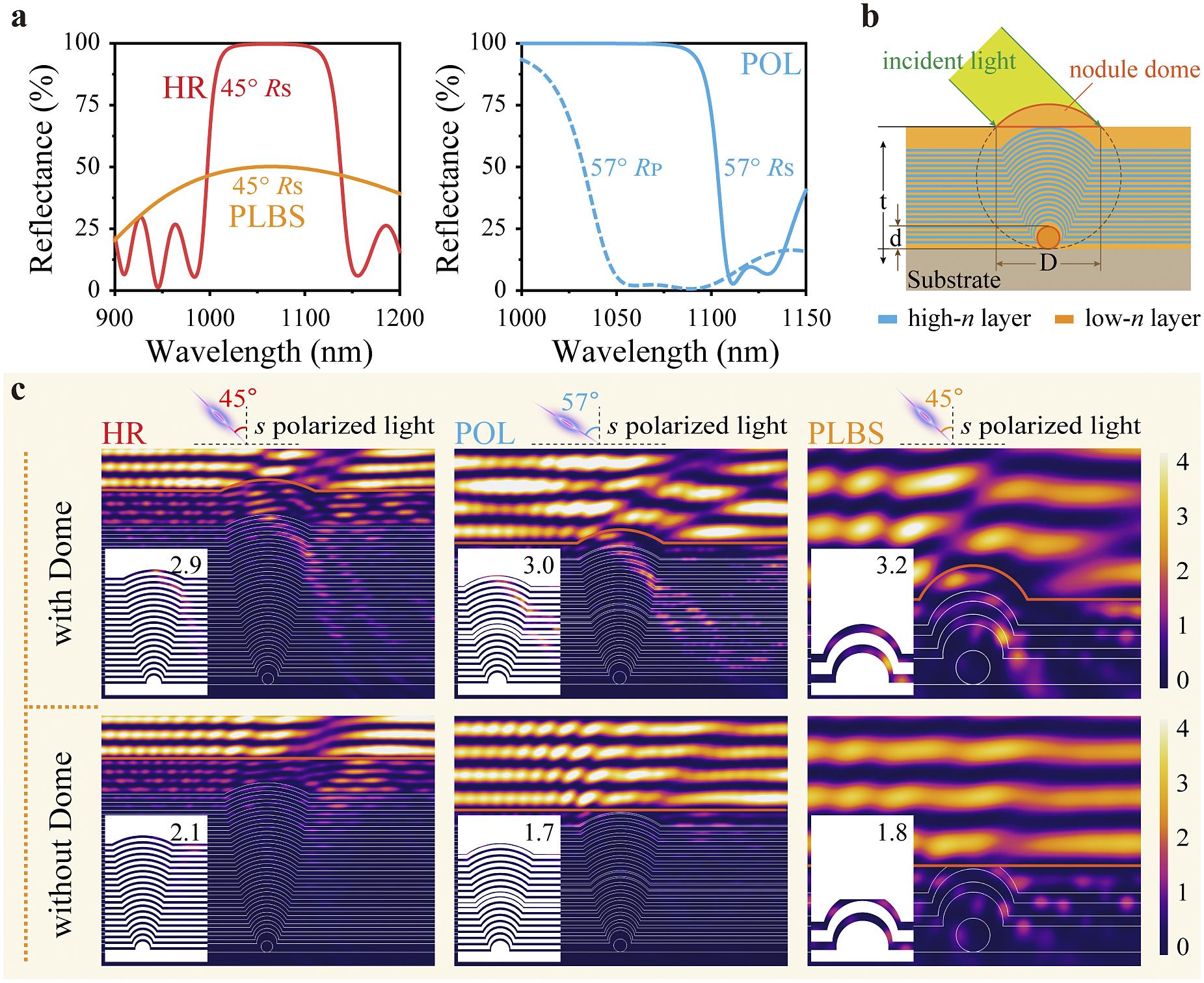
Fig. 1. (a) Theoretical reflectance spectra of a mirror coating (with an incident angle of 45°), a plate laser beam splitter coating (with an incident angle of 45°) and a polarizer coating (with an incident angle of 57°). (b) Geometry of the D = sqrt (4dt ) nodule. (c) Simulated E-field distributions for the nodules with and without domes (with an incident light with a wavelength of 1064 nm). The inset shows the E-field distribution in high-n layers, and the peak E-field intensity values are given.
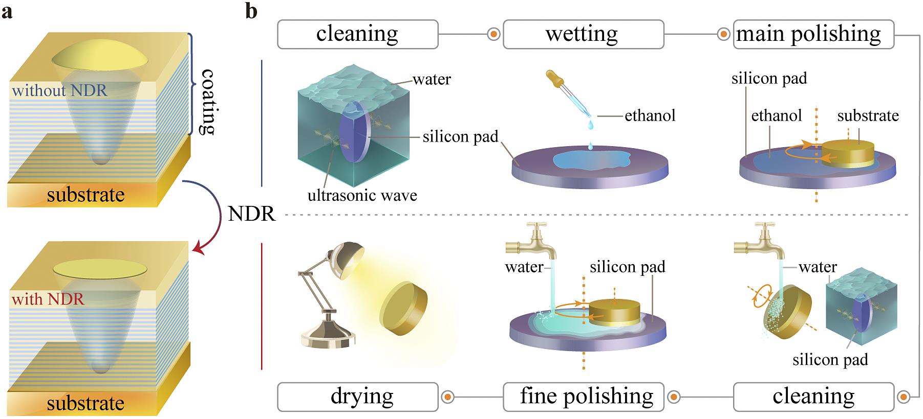
Fig. 2. Schematic illustration of the proposed NDR process. (a) A nodule defect without and with the NDR process. (b) The six steps of the NDR process.
Fig. 3. Morphologies and optical properties of mirror coatings without and with the NDR process. (a) SEM characterized morphologies of the nodule domes with different polishing times. (b) AFM characterized morphologies of the mirror coating with different polishing times. (c) Residual height of the nodule dome versus polishing time. (d) RMS roughness, (e) reflectance spectra (measured at an incident angle of 45°, s-polarized light) and (f) surface figure of the mirror coating without and with the NDR process. Error bars in (c) and (d) describe the values measured at different areas of the coating.
Fig. 4. Laser-induced damage probability. Single-pulse damage probability as a function of the input fluence for (a) all mirror coatings without the NDR process, mirror coatings deposited on substrates with (b) no artificial nodule defects and artificial nodule defects with seed diameters of (c) 200 nm, (d) 550 nm, (e) 750 nm and (f) 1000 nm. Error bars describe the relative error of damage probability, including sample-to-sample uncertainty, measurement error of the laser spot area and fluctuations in laser energy[33].
Fig. 5. Morphologies of nodules (seed diameter: 550 nm) in the coating without the NDR process. (a) Surface and cross-sectional morphologies of a nodule. Surface and cross-sectional morphologies at the nodules after laser irradiation with fluences of (b) 2.8 J/cm2, (c) 3.9 J/cm2 and (d) 5.6 J/cm2. (e) The E-field intensity distribution in high-n layers. (f)–(h) Schematic diagram of the simulated damage morphologies for increasing laser fluence.
Fig. 6. Morphologies of nodules (seed diameter: 550 nm) in the coating with the NDR process. (a) Surface and cross-sectional morphologies of a nodule. Surface and cross-sectional morphologies at the nodules after laser irradiation with fluences of (b) 8.9 J/cm2, (c) 14.3 J/cm2 and (d) 17.5 J/cm2. (e) The E-field intensity distribution in high-n layers. (f)–(h) Schematic diagram of the simulated damage morphologies for increasing laser fluence.
Fig. 7. Simulated E-field distributions and damage morphologies of nodules in coatings without and with the NDR process. (a) Simulated E-field distributions and (b) typical damage morphologies of nodules in coatings without the NDR process. (c) Simulated E-field distributions and (d) typical damage morphologies of nodules in coatings with the NDR process. Insets show the E-field distribution in high-n layers around the micro-crack and the damage area.
| |||||||||||||||||||||||||||||||||||||
Table 1. Design structures of the coatings.
| ||||||||||||||||||||||||||||||||||||||||||||||||||||||||||||||||||||||||||||||||||||||||||
Table 2. Extracted defect parameters of mirror coatings without and with the NDR process.
| |||||||||||||||||||||||||||||||||||
Table 3. Maximum E-field intensity values for nodules with different seed diameters.


Set citation alerts for the article
Please enter your email address

© Copyright 2018-2021 | Chinese Laser Press. All Rights Reserved 沪ICP备15018463号-20