
Yuchan Zhang, Qilin Jiang, Mingquan Long, Ruozhong Han, Kaiqiang Cao, Shian Zhang, Donghai Feng, Tianqing Jia, Zhenrong Sun, Jianrong Qiu, Hongxing Xu. Femtosecond laser-induced periodic structures: mechanisms, techniques, and applications[J]. Opto-Electronic Science, 2022, 1(6): 220005
- Opto-Electronic Science
- Vol. 1, Issue 6, 220005 (2022)
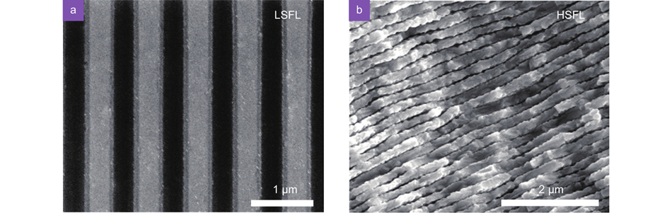
Fig. 1. Scanning electron microscopy (SEM) images of (a ) LSFLs on silicon8, and (b ) HSFLs on ZnSe induced by 800 nm femtosecond laser. Figure reproduced with permission from: (a) ref.8, Optica Publishing Group, under the Optica Open Access Publishing Agreement; (b) ref.9, American Physical Society.
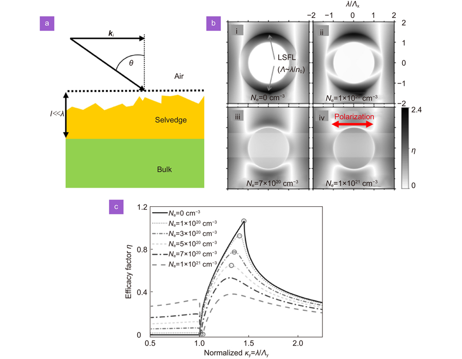
Fig. 2. (a ) The schematic of light irradiated on a rough surface at an incident angle θ, where k i is the wave-vector component parallel to the surface, and l is the thickness of selvedge region. (b ) The efficacy factor η as a function of the normalized LIPS wave vector for silica at different excited state. (c ) The efficacy factor η along the positive ky-axis for silica at different excitation levels, with circles marking ky-positions where LIPS formation could be expected. Figure reproduced with permission from: (a) ref.16, American Physical Society; (b, c) ref.22, AIP Publishing.
Fig. 3. (a ) Schematic illustration of SPPs. (b ) Dispersion curves of SPPs and light in air. (c ) SPP excitation on ZnO surface in the excited state launched by a groove. (d ) The SEM image of the nanostructures on the ZnO surface irradiated by 800 nm femtosecond laser, where the LSFLs originated from the nanogroove or the ablation edge, as shown as the red arrows. Figure reproduced with permission from: (b) ref.49, AIP Publishing; (c, d) ref.21, American Chemical Society.
Fig. 4. (a ) SEM image of HSFLs inside fused silica induced by 800 nm femtosecond laser pulses. (b ) Nanoplasma growth into plane governed by local field distribution, where E pol and E eq are the local fields on the polar axis and in the equatorial plane, respectively4, 20. Figure reproduced with permission from: (a) ref.20, American Physical Society.
Fig. 5. OM images of silicon surface irradiated by a single 800 nm femtosecond pulse of 0.18 J/cm2. The double arrows in (a ) show the laser polarization direction. Figure reproduced with permission from ref.52, Optica Publishing Group, under the Optica Open Access Publishing Agreement.
Fig. 6. Evolution of LSFLs formed on Au film irradiated by a single 800 nm laser pulse with a fluence of 1.96 J/cm2. The laser polarization, E , is perpendicular to the prefabricated nanogroove. Figure reproduced with permission from ref.25, American Physical Society.
Fig. 7. LSFL periods as a function of laser fluence F. The black squares and error bars show the experimental data, and the red curve shows the theoretical values. Figure reproduced with permission from ref.25, American Physical Society.
Fig. 8. (a –b ) SEM pictures of LSFLs induced by the shaped pulse trains with an interval of 16.2 ps. (c ) The cross section of LSFLs. (d ) The 2D fast Fourier transform of (b). (e ) Spectra of the 2D Fourier transform along the x-axis. Figure reproduced with permission from ref.8, Optica Publishing Group, under the Optica Open Access Publishing Agreement.
Fig. 9. SEM images of composite LIPSs prepared by three-beam interference. The insets show the polarization combinations of the three laser beams. Figure reproduced with permission from ref.37, under a Creative Commons Attribution 4.0 International License.
Fig. 10. (a ) SEM images of nanosquares , and (b ) the cross section of nanogratings . (c ) Curvature and separation control of nanogrooves fabricated by 800 nm femtosecond laser with polarization control. (d ) SEM and AFM images of curved single nanogroove on silicon surface induced by 800 nm femtosecond laser with orthogonally polarized dual beams. Figure reproduced with permission from: (a, b) ref.136, under Optica Open Access Publishing Agreement; (c) ref.139, under a Creative Commons Attribution 4.0 International License; (d) ref.27, American Chemical Society.
Fig. 11. Structural colors of “Chinese knot” pattern made up of LSFLs fabricated by a shaped pulse of 16.2 ps on Si surface under different diffraction angles. The inset shows an SEM image of regular LSFLs. Figure reproduced with permission from ref.8, Optica Publishing Group, under the Optica Open Access Publishing Agreement.
Fig. 12. (a -c ) Imaging of anisotropic nanostructures and 5D optical data storage in fused silica153, 155. (a ) Image of the slow axis azimuth of voxels, where the pseudo-color represents the slow axis azimuth. (b ) SEM image of the nanolamella-like structure after polishing and KOH etching. (c ) The enlarged area in the dashed square in (b). (d ) The birefringent images of data voxels of different layers in a 100-layer 5D optical data storage in fused silica after removing the background. Insets are enlargements of small region (10 μm × 10 μm). (e ) Polar diagram of the measured retardance and azimuth of all voxels in (d). Figure reproduced with permission from: (a-c) ref.153, Optica Publishing Group, under the Optica Open Access Publishing Agreement; (d, e) ref.155, under a Creative Commons Attribution License.
Fig. 13. (a ) SEM image of composite nanostructures on ZnSe crystal. (b ) The photoluminescence (PL) spectra of the plane surface and composite nanostructures irradiated by 1200 nm femtosecond laser. Insets (i) and (ii) show PL images of the nanostructures and plane surface, respectively. Figure reproduced with permission from ref.175, AIP Publishing.
Fig. 14. (a –b ) Schematic illustrations of the laser-induced structure in the ITO thin film on the substrate, and the resistivity measured longitudinally (IL) or transversely (IT) along the LIPS direction. (c ) Microscopic configuration of the four-point probe measurement with the probes longitudinal (Micro-L) or transverse (Micro-T) aligned with the LIPSs. (d ) and (e ) are the I-V curves of the anisotropic resistivity surface and the unidirectional resistivity surface measured by the Micro-L or Micro-T method, respectively. Figure reproduced with permission from ref.41, under a Creative Commons Attribution License.


Set citation alerts for the article
Please enter your email address

© Copyright 2018-2021 | Chinese Laser Press. All Rights Reserved 沪ICP备15018463号-20