
Yingjie Zhao, Shan Li, Huixue Ren, Shaojie Li, Peide Han. Energy band adjustment of 808 nm GaAs laser power converters via gradient doping[J]. Journal of Semiconductors, 2021, 42(3): 032701
- Journal of Semiconductors
- Vol. 42, Issue 3, 032701 (2021)
Abstract
1. Introduction
Following the introduction of the concept of a space-based solar power station, wireless energy transmission has once again entered our field of vision. Wireless energy transmission is mainly divided into microwave wireless energy transmission and laser wireless energy transmission. Due to the excellent directivity of lasers, low transmission loss, lack of electromagnetic interference during energy transmission, and compactness of the receiving device, laser wireless energy transmission has potential applications in various fields, such as precision instrument manufacturing and aerospace[
To match the material band gap with the laser wavelength, numerous semiconductor materials have been used for different laser wavelength, such as GaAs for 808 nm laser light, InGaAs[
In addition to the conventional structure[
![]()
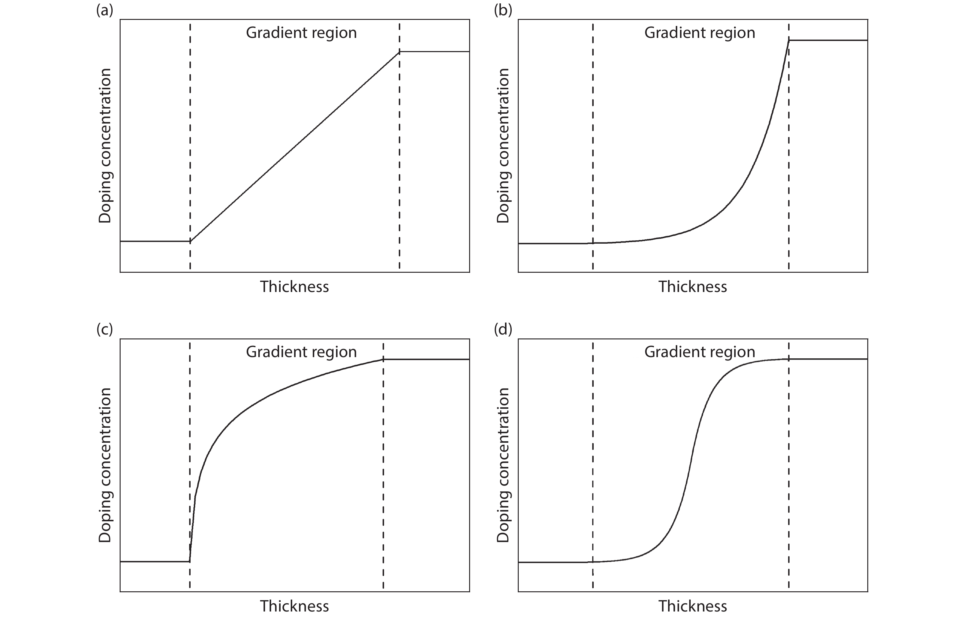
Figure 1.The shapes of gradient doping structure. (a) Linear gradient doping. (b) Exponential gradient doping. (c) Logarithmic gradient doping. (d) Smooth gradient doping.
2. Theory and structure
Owing to their epitaxial characteristics, the previously used LPCs all possess a uniform doping structure, therefore, the energy bands outside of the PN junction are approximately flat. Consequently, the photogenerated carriers generated in these regions are mainly transported via diffusion, which is very inefficient. Furthermore, those carries cannot be separated by diffusion along, resulting in severe recombination in this area. By introducing gradient doping regions into the conventional structure, the energy band can be adjusted purposefully, and forming a stable electric field in the gradient doping region[
To achieve the effect of improving the carrier transport, the energy band needs to be continuously tilted downward from the emitter layer to the base layer[
![]()
Figure 2.(Color online) Structures of GaAs LPCs with different position of gradient doping region.
3. Method and discussion
3.1. Simulation method
Silvaco TCAD was used to numerically simulate the structures mentioned above. From a mathematical point of view, there are thousands of specific doping methods for each structure. For calculation convenience and efficiency, we have simplified the discussion process. From the distribution of the recombination rate of the traditional structure (Fig. 3) we know that, the recombination of the base layer is mainly concentrated away from the junction region. When the gradient doping region in the base layer is near the junction region (Figs. 2(a) and 2(b)), the electric field generated by it cannot be effectively applied to the position with a higher recombination rate. Therefore, in theory, only when the gradient doping region is located away from the junction (Figs. 2(c) and 2(d)), can it effectively reduce the recombination rate, so we only need to discuss this structure later. But for emitter layer, the thickness of the emitter is relatively thin, the electric field generated by the window layer and the junction can extend to the inside of the emitter layer to a certain extent, so it is arduous to infer the optimal position of the gradient doping region in the emitter layer. As a result, both structures near and away from the junction region need to be discussed.
![]()
Figure 3.Distribution of recombination rate in traditional structure of GaAs LPCs.
Therefore, the specific discussion method is: In the case where the entire base layer is doped gradually, the optimal doping concentration on the front (the incident surface of the laser) and back surfaces of the gradient doping region is determined first. Subsequently, the optimal thickness of gradient doping region in the base layer (the gradient doping region is away from the PN junction of LPC) is determined by simulation, until now the optimal doping parameters of the base region are maintained. Then, the emitter layer is discussed in the same way, and finally, the best gradient doping structure is determined. (To avoid band offset, the doping concentration of the non-gradually doping region on the front or back side of the gradient doping region is the same as that of the front or back surface of the gradient doping region, as shown in Fig. 1.) Based on the structure that we previously used, taking into account the actual situation and simplifying the discussion process, the doping concentration on the front surface (for convenience, we call it surface EF) of the gradient doping region in the emitter layer and the doping concentration on the back surface (for convenience, we call it surface BB) of the gradient doping region in the base layer are tentatively fixed at 1 × 10¹⁷ and 5 × 1018 cm–3, respectively[
3.2. Optimization of the linear gradient doping structure
The simulation results of the base layer of linear gradient doping LPC are shown in Fig. 4. When the entire base layer is doped gradually, as the doping concentration on the front surface gradually decreases (the difference between the doping concentration of front and back surface gradually increases), the photoelectric conversion efficiency of LPC first increases and then decreases (Fig. 4(a)). The highest efficiency is obtained when the doping concentration on the front surface is 3 × 1016 cm–3. This is because as the doping concentration on the front surface of the gradient doping region decreases, the internal electric field in the base layer increases (Fig. 5(a)), which facilitates the separation and transport of photogenerated electron–hole pairs generated here, The reduction recombination rate of the base layer (Fig. 5(b)), which in turn contributes to the improvement of VOC and FF of LPC. At the same time,
![]()
Figure 4.(Color online) Simulation results of the base layer of linear gradient doping LPC. (a) Simulation about doping concentration when the gradient doping region thickness (GDT) in base layer is 1.5, 2.5, and 3.5
![]()
Figure 5.(Color online) (a) Distribution of electric field in base layer with different front surface doping concentration. (b) Distribution of recombination rate in base layer with different front surface doping concentration.
where VD is the contact potential difference of the PN junction, k0 is the Boltzmann constant, T is the temperature, q is the electronic charge, ND and NA is the doping concentration of N and P region, ni is the intrinsic carrier concentration. It can be known from Eq. (1) that when the doping concentration on the front surface of the gradient doping region decreases, the electric field intensity and the potential difference VD of the junction region will decrease accordingly, which will lead to an increase in the recombination rate of the junction region and a decrease in the VOC of the device[
To confirm whether the optimal doping concentration on the front surface (For convenience, we call it surface BF) of gradient doping region in the base layer will change due to the change of the thickness of the gradient doping region, we also simulate it when the thickness of gradient doping region is 1.5 and 2.5 μm, respectively. The simulation result is shown in Fig. 4(a). It can be seen that the thickness of the gradient doping region does not affect the optimal doping concentration.
When the doping concentration on the front and back surfaces of the gradient doping region is unchanged, as the thickness of the gradient doping region decreases, the gradient of doping concentration in the gradient doping region gradually increases, and the internal electric field will gradually increase. And the photogenerated electron–hole pairs generated here will be more efficiently separated and transported. Therefore, the reduction of the thickness of the gradient doping region is beneficial to the reduction of the recombination rate inside the gradient doping region. But at the same time, the thickness of the non-gradient doping region will increase accordingly. Since there is no electric field in the non-gradient doping region, the recombination rate is relatively high. In other words, as the thickness of the gradient doping region gradually decreases, the overall recombination rate of the base layer will first decrease and then increase, which is obviously reflected in Fig. 4(b). With the gradual increase in the thickness of the gradient doping region of the base layer, the efficiency of LPC increases first and then decreases. The maximum efficiency is obtained when the thickness of the gradient doping region is 2.3 μm.
After the optimal structure of the base layer is obtained, the simulation results for the emitter layer are shown in Fig. 6. When the doping concentration on the back surface (for convenience, we call it surface EB) of the emitter layer is 5 × 1016 cm–3, and the thickness of the gradient doping region is 0.9 μm (the gradient doping region is close to the PN junction), the highest efficiency obtained is 56.29%.
![]()
Figure 6.(Color online) Simulation results of the emitter layer of linear gradient doping LPC. (a) Simulation about doping concentration when the entire emitter layer is doped gradually. (b) Simulation about the thickness of gradient doping region in different position.
Since the doping concentration of surface EF and surface BB is tentatively fixed at 1 × 10¹⁷ and 5 × 1018 cm–3 before, in order to obtain the optimal doping concentration of them, after the optimal structure of linear gradient doping LPC is determined, we have carried out the simulation under the condition that the thickness and position of gradient doping region are unchanged. The specific simulation method is: The optimal doping concentration of surface BB is determined first, and then optimal doping concentration of surface BF is determined by simulation. As mentioned earlier, the optimal doping concentration of the gradient doping region is independent of the thickness, so there is no need to discuss the thickness of the gradient doping region at this time; then the optimal doping concentration of surface EF and surface EB will be obtained by the same method. The simulation results are shown in Fig. 7. When the doping concentration on the surface EF, EB, BF and BB are 7 × 10¹⁷, 3 × 10¹⁶, 3 × 10¹⁶ and 2 × 1018 cm–3, respectively, the highest efficiency obtained is 57.22%.
![]()
Figure 7.Simulation about doping concentration on the (a) back and (b) front surface of the gradient doping region in base layer. Simulation about doping concentration on the (c) front and (d) back surface of the gradient doping region in emitter layer.
3.3. Optimization of the exponential gradient doping structure
From the simulation results (Figs. 8 and 9) for exponential gradient doping structure (for the convenience of comparison, the doping concentration on surface EF and surface BB of exponential gradient doping structure are fixed at 7 × 10¹⁷ and 2 × 1018 cm–3, respectively) we know that, because this kind of gradient doping method and linear gradient doping are the same in the mechanism of improving the performance of LPC, the change trends of these two are similar. When the doping concentration on the surface BF is 6 ×1016 cm–3 and the thickness is 3.4 μm; when the doping concentration on the surface EB is 9 × 1016 cm–3 and the thickness is 1.1 μm, and the gradient doping region is near the junction, the highest efficiency obtained is 57.65%.
![]()
Figure 8.(Color online) Simulation results of the base layer of exponential gradient doping LPC. (a) Simulation about doping concentration when the entire base layer is doped gradually. (b) Simulation about the thickness of gradient doping region
![]()
Figure 9.(Color online) Simulation results of the emitter layer of exponential gradient doping LPC. (a) Simulation about doping concentration when the entire emitter layer is doped gradually. (b) Simulation about the thickness of gradient doping region in different position.
Due to the change rate of doping concentration of exponential gradient doping in the depth of the gradient doping region is significantly higher than the linear gradient (Fig. 1), in the depth of the gradient doping region, the exponential gradient can generate a larger electric field[
![]()
Figure 10.(Color online) (a) Distribution of electric field in base layer of linear and exponential gradient doping LPCs. (b) Distribution of recombination rate in base layer of linear and exponential gradient doping LPCs.
4. Conclusion
Through the numerical simulation of LPC with different structures using two shapes of gradient doping methods, linear gradient, and exponential gradient, it is confirmed that the gradient doping method can effectively improve the separation and transport capacity and reduce the recombination rate of photogenerated carriers in the gradient doping region. Furthermore, the photoelectric conversion efficiency of LPC is improved. At the same time, compared to the linear gradient, the improvement of efficiency of the exponential gradient doping structure is more obvious. For exponential gradient doping structure, when the doping concentration of surface BF and surface BB are 6 × 10¹⁶ and 2 × 1018 cm–3, respectively, the thickness is 3.4 μm, and the gradient doping region is away from the junction region; the doping concentration of surface EF and surface EB are 7 × 10¹⁷ and 9 × 1016 cm–3, respectively, and the thickness is 1.1 μm, and the gradient doping region is close to the junction region, an efficiency of 57.65% is obtained.
Acknowledgements
This work was supported by the National Key R&D Program of China (No. 2018YFB1500500) and also supported by Ally Fund of Chinese Academy of Sciences (No. Y072051002).
References
[1] C Guan, W Liu, Q Gao. Influence of the mesa electrode position on monolithic on-chip series-interconnect GaAs laser power converter performance. Mater Sci Semicond Process, 75, 136(2018).
[2] V Andreev, V Khvostikov, V Kalinovsky et al. High current density GaAs and GaSb photovoltaic cells for laser power beaming. Proceedings of 3rd World Conference on Photovoltaic Energy Conversion, 761(2003).
[3] A Fave, A Kaminski, M Gavand et al. GaAs converter for high power laser diode. Conference Record of the Twenty Fifth IEEE Photovoltaic Specialists Conference, 101(1996).
[4] C Guan, L Li, H M Ji et al. Fabrication and characterization of a high-power assembly with a 20-junction monolithically stacked laser power converter. IEEE J Photovolt, 8, 1355(2018).
[5] J W Shi, F M Kuo, C S Yang et al. Dynamic analysis of cascaded laser power converters for simultaneous high-speed data detection and optical-to-electrical DC power generation. IEEE Trans Electron Devices, 58, 2049(2011).
[6]
[7] N A Kalyuzhnyy, V M Emelyanov, S A Mintairov et al. InGaAs metamorphic laser (λ = 1064 nm) power converters with over 44% efficiency. InAIP Conference Proceedings, 2012, 110002(2018).
[8] M A Green, J Zhao, A Wang et al. 45-percent efficient silicon photovoltaic cell under monochromatic light. IEEE Electron Device Lett, 13, 317(1992).
[9] S D Jarvis, S J Sweeney, M Perren et al. Development and characterisation of laser power converters for optical power transfer applications. IET Optoelectron, 8, 64(2014).
[10] V P Khvostikov, S V Sorokina, O A Khvostikova et al. GaSb laser-power (λ = 1550 nm) converters: Fabrication method and characteristics. Semiconductors, 50, 1338(2016).
[11] S Fafard, M C A York, F Proulx et al. Ultrahigh efficiencies in vertical epitaxial heterostructure architectures. Appl Phys Lett, 108, 071101(2016).
[12] D Krut, R Sudharsanan, W Nishikawa et al. Monolithic multi-cell GaAs laser power converter with very high current density. Conference Record of the Twenty-Ninth IEEE Photovoltaic Specialists Conference, 908(2002).
[13] J Schubert, E Oliva, F Dimroth et al. High-voltage GaAs photovoltaic laser power converters. IEEE Trans Electron Devices, 56, 170(2009).
[14] C Algora, V Diaz. Performance and optimization of monochromatic p/n heteroface AlGaAs/GaAs photovoltaic cells. Solid-State Electron, 41, 1787(1997).
[15] T Q Shan, X L Qi. Design and optimization of GaAs photovoltaic converter for laser power beaming. Infrared Phys Technol, 71, 144(2015).
[16] V P Khvostikov, S V Sorokina, N S Potapovich et al. Modification of photovoltaic laser-power (λ = 808 nm) converters grown by LPE. Semiconductors, 52, 366(2018).
[17] S T Hwang, T Hwang, S Lee et al. Selective rear contact for Ga0.5In0.5P- and GaAs-based solar cells. Sol Energy Mater Sol Cells, 182, 348(2018).
[18] Y Zhao, P Liang, H Ren et al. Enhanced efficiency in 808 nm GaAs laser power converters via gradient doping. AIP Adv, 9, 105206(2019).
[19] S T Hwang, S Kim, H Cheun et al. Bandgap grading and Al0.3Ga0.7As heterojunction emitter for highly efficient GaAs-based solar cells. Sol Energy Mater Sol Cells, 155, 264(2016).
[20]
[21]

Set citation alerts for the article
Please enter your email address
© Copyright 2018-2021 | Chinese Laser Press. All Rights Reserved 沪ICP备15018463号-20