• Acta Photonica Sinica
  • Vol. 53, Issue 2, 0212002 (2024)
Shengshuo CHEN, Yansong LI*, Dongxu CHEN, Shijia KANG, Zhiguang XU, and Jun LIU
Author Affiliations
  • School of Electrical and Electronic Engineering,North China Electric Power University,Beijing 102206,China
  • show less
    DOI: 10.3788/gzxb20245302.0212002 Cite this Article
    Shengshuo CHEN, Yansong LI, Dongxu CHEN, Shijia KANG, Zhiguang XU, Jun LIU. Temperature Compensation Method for Optical Voltage Sensing Based on Temperature Field and D-Kalman Parameter Estimation[J]. Acta Photonica Sinica, 2024, 53(2): 0212002 Copy Citation Text show less
    Schematic of horizontal modulation OVS
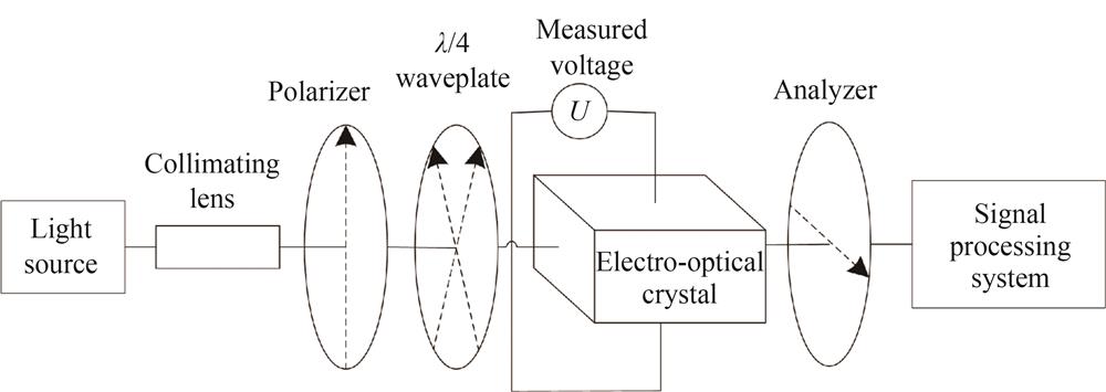
    Fig. 1. Schematic of horizontal modulation OVS
    Internal structure section of OVS sensing head
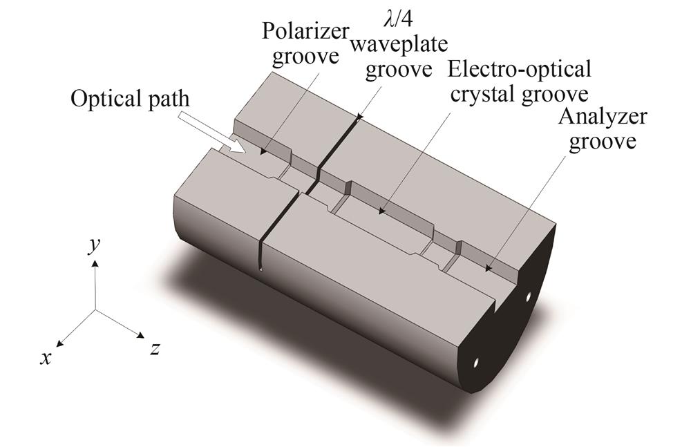
    Fig. 2. Internal structure section of OVS sensing head
    BGO crystal thermal model
    Fig. 3. BGO crystal thermal model
    Schematic of external temperature change
    Fig. 4. Schematic of external temperature change
    Coordinate system definition of stage II temperature field
    Fig. 5. Coordinate system definition of stage II temperature field
    Construction of BGO crystal thermal circuit model
    Fig. 6. Construction of BGO crystal thermal circuit model
    Flow of central differential Kalman filtering
    Fig. 7. Flow of central differential Kalman filtering
    Temperature fitting image of BGO crystal physical properties parameters
    Fig. 8. Temperature fitting image of BGO crystal physical properties parameters
    Simulation of BGO crystal temperature field
    Fig. 9. Simulation of BGO crystal temperature field
    Model calculation and simulation comparison of BGO crystal face center point and body center point
    Fig. 10. Model calculation and simulation comparison of BGO crystal face center point and body center point
    Cooling environment BGO body center point model calculation and simulation comparison
    Fig. 11. Cooling environment BGO body center point model calculation and simulation comparison
    Temperature-time distribution at each position of the central axis of the BGO crystal
    Fig. 12. Temperature-time distribution at each position of the central axis of the BGO crystal
    The analytical formula of the through optical path and the relative error of the simulation
    Fig. 13. The analytical formula of the through optical path and the relative error of the simulation
    Comparison of the measured data of the temperature of the center point of the crystal surface and the calculated value of the temperature field model
    Fig. 14. Comparison of the measured data of the temperature of the center point of the crystal surface and the calculated value of the temperature field model
    BGO crystal internal temperature estimation result
    Fig. 15. BGO crystal internal temperature estimation result
    Photodetector linear response calibration
    Fig. 16. Photodetector linear response calibration
    The AC and DC components of the sensor output signal in a heating environment
    Fig. 17. The AC and DC components of the sensor output signal in a heating environment
    CDKF estimation results for refractive index n0
    Fig. 18. CDKF estimation results for refractive index n0
    Optical voltage sensor temperature compensation experimental platform equipment
    Fig. 19. Optical voltage sensor temperature compensation experimental platform equipment
    Optical voltage sensor temperature compensation experiment platform connection schematic
    Fig. 20. Optical voltage sensor temperature compensation experiment platform connection schematic
    ParametersFitting equations and evaluation metrics
    Thermal conductivity λ/(W·m-1·K-1Formulaλ=-4.073×10-13T5+9.9×10-10T4-9.428×10-7T3+0.0004466T2-0.1105T+13.95
    IndicatorSSER-squareRMSE
    0.018 20.998 70.067 46
    Specific heat capacity Cp/(J·kg-1·K-1FormulaCp=1.541×10-18T8-5.616×10-15T7+8.654×10-12T6-7.319×10-9T5+3.671×10-6T4-0.00109T3+0.175T2-9.434T+662.7
    IndicatorSSER-squareRMSE
    0.023 5910.108 6
    Thermal diffusivity α'/(10-6·K-1Formulaα'=-1.152×10-11T4+2.176×10-8T3-1.67×10-5T2+0.009191T+4.725
    IndicatorSSER-squareRMSE
    0.003 8480.999 30.025 32
    Table 1. Fitting formula and evaluation index of physical properties parameters
    ParametersValue
    Poisson's ratio μ0.175
    Convective heat transfer coefficient h2.5 W·m-2·K-1
    Elasto-optical coefficient p11-p12-2.995×10⁻¹³ m2·N-1
    Elasto-optical coefficient p44-1.365×10⁻¹² m2·N-1
    Crystal length l10 mm
    Crystal thickness d5 mm
    Table 2. Model parameters
    ParametersThermal resistance RThermal capacity C
    Value1 604.708 82.297 2
    Table 3. Thermal path model parameters
    Temperature/℃Compensation voltage /kV
    202.984 4
    252.989 8
    303.014 4
    352.990 1
    403.011 1
    Table 4. Calculation results of voltage compensation at different external temperatures
    Temperature/℃D-KalmanBPNN
    200.52%0.96%
    250.34%0.79%
    300.48%0.66%
    350.33%0.82%
    400.37%0.91%
    Table 5. Comparison of relative errors of different temperature compensation methods under the same platform
    Temperature rangeCompensation methodsCompensation results
    [20 ℃,40 ℃]D-Kalman0.52%
    [-10 ℃,50 ℃]Fresnel rhombic crystal0.9%
    [20 ℃,30 ℃]Reciprocal optical path1.53%
    Table 6. Comparison of relative errors of different temperature compensation methods for different platforms
    EquipmentManufacturerModel
    Light sourceFIBKEY6 900 Series Handheld Light Source
    PhotodetectorTHORLABSPDA36A2
    High frequency transformerYangzhou Pengxiang Electric Power Equipment FactoryPX1007
    Fluorescent fiber thermometerINDIGOFOTS-DINA-7060-N
    Table 7. Experimental equipment model
    Shengshuo CHEN, Yansong LI, Dongxu CHEN, Shijia KANG, Zhiguang XU, Jun LIU. Temperature Compensation Method for Optical Voltage Sensing Based on Temperature Field and D-Kalman Parameter Estimation[J]. Acta Photonica Sinica, 2024, 53(2): 0212002
    Download Citation