
Zhongjun Jiang, Yingjian Liu, Liang Wang. Applications of optically and electrically driven nanoscale bowtie antennas[J]. Opto-Electronic Science, 2022, 1(4): 210004
- Opto-Electronic Science
- Vol. 1, Issue 4, 210004 (2022)
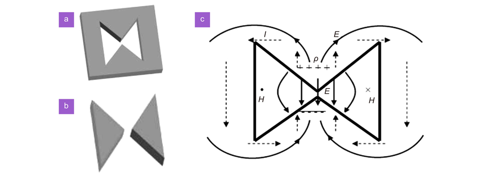
Fig. 1. Bowtie apertured (a ) and gaped (b ) antennas. (c ) Induced surface charges and electric dipole when incident electric field polarizes along the tips. Figure reproduced with permission from: (a-b) ref.4, Copyright 2006 American Chemical Society.
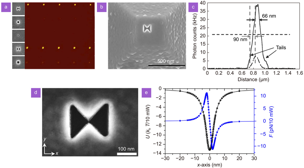
Fig. 2. Near-field imaging and trapping using (apertured) bowties. (a ) Transmission through the subwavelength apertures. Bowtie apertures show much enhanced transmission. Left: different apertures. Right: far-field transmission measurements. (b ) Bowtie apertures fabricated on the SNOM probe. (c ) Line profiles of SNOM images using bowtie (solid line) and square (dashed line) aperture probes. (d ) 5-nm-gap bowtie apertures. (e ) Optical potentials U and the corresponding optical forces F along the x-axis. Figure reproduced with permission from: (a–c) ref.3, Copyright 2007 AIP Publishing; (d–e) ref.27, Copyright 2018 the author(s), under a Creative Commons Attribution 4.0 International License.
Fig. 3. Nonlinear response in bowties. (a ) Three-dimensional (3D) gold bowties array. (b ) Nonlinear emission spectrum from a single bowtie (inset). (c ) Spectrum of generated high harmonics from 2D bowties array (inset). (d ) Experimental (TPPL, circles) and theoretical (field enhancement, squares) results versus bowtie gap size. Inset shows a bowtie with a 22 nm gap. Figure reproduced with permission from: (a) ref.32, American Chemical Society; (b) ref.35, under a Creative Commons Attribution 3.0 License; (c) ref.15, American Physical Society.
Fig. 4. Nanolithography using bowties. (a ) Bowtie apertures with a 30 nm gap. (b ) AFM image of 40 nm × 50 nm lithography hole. (c –d ) AFM image (c) and cross section (d) along the nanoantenna axis of bowties exposed at 25 μW laser power. Feature size of ~30 nm for each of the resist pillars was measured. (e ) SEM image of the fabricated circular contact probe. (f ) AFM image of a 22-nm half pitch resolution line array pattern. (g –h ) Bowtie nanolithography combined with metal-insulator-metal (g) and hyperbolic metamaterials (h). Figure reproduced with permission from: (a, b) ref.4, Copyright 2016 American Chemical Society; (c, d) ref.16, American Chemical Society; (e, f) ref.37, Copyright 2012 John Wiley and Sons; (g) ref.38, Copyright 2019 Optical Society of America; (h) ref.41, IOP Publishing.
Fig. 5. Bowtie based nanosources. (a ) Schematic of 3D bowtie plasmonic lasers. (b ) Evolution of lasing spectra from 3D Au bowties under pump polarization parallel to the tip axis. Inset shows emission intensity versus pump pulse energy density plotted on a semilogarithmic scale. (c ) Directional SP out-coupling emission. (d ) Bowties with a small gap. (e ) Simulated near-field patterns of one of resonant modes in bowties. (f ) Thermal emission spectrum under different bowtie gap sizes. Figure reproduced with permission from: (a–c) ref.17, Copyright 2012 American Chemical Society; (d–f) ref.44, Copyright 2017 the author(s), under the ACS AuthorChoice via CC-BY-NC-ND Usage Agreement .
Fig. 6. 2D materials photodetectors based on bowties. (a ) Schematic and (b ) SEM image of the plasmonically enhanced graphene photodetector. (c ) The magnitude of in-plane electric fields. Strong plasmonic field enhancements in the gap were observed. (d ) Eye diagram of 100 Gbit/s OOK optical signals. (e ) Optical and (f ) SEM image of bowtie gap antennas for high responsivity detectors. (g ) Optical and (h ) SEM image of bowtie aperture antennas for high polarization. Figure reproduced with permission from: (a–d) ref.45, Copyright 2019 The Author(s), under the ACS AuthorChoice Usage Agreement ; (e–h) ref.18, Copyright 2018 American Chemical Society.
Fig. 7. Surface plasmons mediated via the IET process. (a ) Schematic of the Al-AlOx-Au tunnel junction. (b ) Energy level diagram of the IET process. (c ) Bias dependent emission spectra. Emitted photons with cut-off frequencies can be seen. Figure reproduced with permission from ref.49, under a Creative Commons Attribution 4.0 International License.
Fig. 8. Light emission from bowtie antenna based tunnel junctions. (a ) Lateral tunnel junctions made by bowtie gap-antennas. Inset shows that the bowtie antennas are connected before the electro-migration process. (b ) Time evolution of normalized conductance (G/G0). (c ) Light emission spectra. Left column: images captured under different biases. Right column: spectral evolution under different bias. (d ) Enhanced LDOS in the order of 105. Solid line: bowties case. Dashed lines: nanowire case. (e ) Wavelength dependent normalized LDOS (red) and radiation efficiency (black). They both contribute to the ultimate emission spectrum. Figure reproduced with permission from: (a–d) ref.19, Copyright 2019 American Chemical Society; (e) ref.64, Copyright 2020 Optical Society of America.
| ||||||||||||||||||||||||||||||||||||||||||||||||||||||||
Table 1. Comparison on the performance of tunnel junctions

Set citation alerts for the article
Please enter your email address
© Copyright 2018-2021 | Chinese Laser Press. All Rights Reserved 沪ICP备15018463号-20