Abstract
The chromatic aberration of metasurfaces limits their application. How to cancel or utilize the large chromatic dispersion of metasurfaces becomes an important issue. Here, we design Si-based metasurfaces to realize flexible chromatic dispersion manipulation in mid-infrared region. We demonstrate the broadband achromatic metalens and achromatic gradient metasurface to cancel the chromatic aberration over a continuous bandwidth (8–12 μm). In contrast, the metalens and gradient metasurface with enhanced chromatic dispersion have also been realized, where the focal length and deflection angle with different wavelengths vary more significantly than the conventional devices designed with geometric phase. These demonstrations indicate promising potential applications.Metasurfaces are two-dimensional metamaterials, which have various intriguing optical properties and applications[1–4]. Through proper design, the nano-antennas, phase, amplitude, and polarization of the incident light can be well controlled. Phase generation and manipulation are of crucial importance in metasurface designing. The resonant phase that is related to the electromagnetic resonances in the unit element is an important kind of phase in metasurfaces, dependent on the incident wavelengths and geometric parameters of the unit element, such as shape and size[5]. Another commonly used phase is the geometric phase that is related to the orientation of the unit element with circularly polarized incidence. Geometric phase is independent of the shape and size of unit elements, thus leading to a broadband working property[6]. Most of metasurfaces are based on these two kinds of phase generation and manipulation principles.
Sign up for Chinese Optics Letters TOC. Get the latest issue of Chinese Optics Letters delivered right to you!Sign up now
Chromatic dispersion is an important property of optical devices. For normal chromatic dispersion, the refractive index decreases when the wavelength increases, leading to larger focal lengths and smaller deflection angles of prisms with longer wavelengths. The chromatic aberration seriously affects the optical functionalities of the optical devices[7]. In order to improve the performance of full-color optical applications, the researchers developed the concept of achromatic aberration[8,9]. For example, an achromatic objective[10] is composed of the refractive lenses with several kinds of optical materials arranged into a single unit to achieve the same focal length, which completely eliminate chromatic aberration of three or four wavelengths. But, this strategy makes the lenses large, complex, and heavy, which ultimately limits its application and flexibility. Due to their ability to realize wavefront control with high efficiency, dielectric metasurfaces have quite promising applications in imaging, display, detection, etc. However, the chromatic aberration of metasurfaces dramatically limits their applications in multiwavelength or broadband cases. In contrast with conventional optical lenses, planar lenses based on metasurfaces are called metalenses. The dielectric metasurfaces for metalenses[11] greatly reduce the loss and improve the focusing efficiency. Besides, the dielectric metalens can realize a high numerical aperture (NA)[8] through properly designing the metasurface unit elements, which have been realized from the visible region[11,12], the near-infrared region[13,14], and the mid-infrared region[15,16] to the terahertz region[17]. Some pioneering works have suggested that achromatic metalenses working at certain discrete wavelengths or in a narrow wavelength bandwidth can be achieved[18–20]. However, these metalenses with limited chromatic dispersion manipulation are not competent enough for full-color imaging applications. Our work focuses on bandwidth chromatic dispersion manipulation of metasurface devices in the transmission mode, which is achieved by merging an integrated resonant unit element with the geometric phase method. It can not only achieve the effect of wide-band achromatic aberration, but also enhance chromatic dispersion, realizing the flexible control of chromatic dispersion. These demonstrations pave the way toward the realization of broadband chromatic dispersion manipulation flat optical devices and have broad application prospects. In particular, the mid-infrared region is interesting for practical applications in imaging and spectroscopy. Recently, various mid-infrared metasurface-based devices have been reported, including metalenses[16,21,22], modulators[23], polarization controllers[24], perfect absorbers[25], thermal emitters[26], and infrared sensors[27].
Here, we will focus on chromatic dispersion manipulation based on metasurface devices in the mid-infrared region. The first example is chromatic aberration control for achromatic lenses operating over a continuous bandwidth. The second example is the design of a broadband achromatic gradient metasurface, which is able to transmit broadband light by the same angle. The third example is a metalens with super dispersion, where the focal length decreases as the wavelength increases, and the dispersion effect is greater than that of conventional diffractive lenses. We also design a broadband super-chromatic gradient metasurface, and, with the wavelength change from 8 to 12 μm, the angle is changed from 33.36° to 23.1°, respectively. Our results will pave the way toward a realization of broadband flat optical elements, laying an important basis for future applications, such as imaging[28,29], spectroscopy[30], color holograms[31], polarizers[32], and optical metamixer[33], as well as beam deflection[34–37].
Our main goal is to maximize the compensation phase coverage and optimize the parameters of nanopillars. Phase compensation of the selected units can enable broadband chromatic dispersion manipulation metasurfaces devices (Table 1 in Supplementary Materials). These simulations are realized by using CST Microwave Studio. In the design of unit elements, a unit-cell boundary condition is used to simulate the transmission spectrum and phase profile in an array structure. In the design of the metalens, cylindrical lenses are simulated to simply evaluate the focal length of each metalens, which is carried out using the open boundary condition in the and directions and periodic boundary conditions in the direction. As for the gradient metasurfaces, the boundary condition is the same.
The designed phase of chromatic dispersion manipulation metasurface devices can be divided into two parts. The first component is a basic phase profile without dispersion and only related with position, while the other one is dependent on the wavelength, which is called the compensation phase. The former one is directly obtained using geometric phase via rotating the unit elements, while the latter one is realized with integrated resonances. Phase compensation is the phase difference as a function of wavelength, which is offered from the integrated resonant unit element. Each selected structure is determined according to the phase compensation, and the rotation angle of the corresponding structure is determined according to the basic phase.
Figure 1(a) shows a schematic of the broadband achromatic metalens, which focuses different incident wavelengths to a single spot. The system consists of a Si metasurface on a sapphire substrate. The metasurfaces are composed of arrays of high-index dielectric Si nanopillars with different sizes.

Figure 1.Achromatic metalens. (a) The schematic of the broadband achromatic metalens. As the incident wavelength changes, the focal point remains focused at the same spot. (b) The phase profile of the broadband achromatic metalens at the working wavelength.
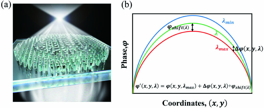
The required phase profile for a metalens can be described by the equation as follows[11]: where and are the designed wavelength and focal length, respectively, and are the in-plane coordinates of arbitrary position in the metalens. In order to achieve a specially designed metalens, additional phase shifts need to be introduced, which is schematically shown in Fig. 1(b). The phase profile of the achromatic metalens is is chosen to be wavelength dependent. , with and , where , are the boundaries of the working wavelength, respectively, and is the largest additional phase shift between and of the lens’ central position. Here, our working wavelength region is from 8 to 12 μm.
By using the phase division approach, Eq. (2) can be rewritten as
The phase difference is is independent of the working wavelength and only related with position, and it can be obtained by the geometric phase via rotating the unit elements. is the compensation phase that is a function of both working wavelength and position. The required compensation phase is inversely proportional to , which can be obtained by specially designed unit elements. Because the two phases come from different generation mechanisms, they will not affect each other, and they can be directly added together[13].
Figure 2(a) shows the circularly polarized conversion efficiency (dark curves) and phase response (blue curve) for the building blocks of our achromatic metalens. The gray area corresponds to the wavelengths of interest for 8–12 μm. The phase compensation can enable a broadband achromatic metalens with different sizes (Table 1 in Supplementary Materials). In Fig. 2(a), the phase and transmission efficiency of a specially designed nanopillar are shown with the phase difference between and within the working bandwidth, with phase compensation being 770°. Each unit element is comprised of different nanopillars [Fig. 2(a), inset]. Phase and transmission efficiency of other unit elements are shown in Fig. 1 of Supplementary Materials. The Si nanopillars present high-order resonance, similar to a waveguide resonator. The main factor of phase delay is the waveguide. Due to these resonant modes, the transmission efficiency is high, and its peak can be up to 97.7%, with the average efficiency at about 60% over the whole working bandwidth. It can be seen from Fig. 2(a) that the phase dispersion owns a linear relation with . These nanopillars are carefully chosen and specially rotated considering their positions (). The electric-field distributions of the Si nanopillars are shown in Fig. 2(b). The height of all Si nanopillars is fixed at , standing on an substrate. The induced optical fields are highly concentrated inside the dielectric structures, resulting in the weak optical coupling between dielectric nanopillars. If the period of the unit element reduces or the unit element changes to metallic structures, which has large radiation and field distribution outside the structure, the coupling has to be considered.
Figure 2.Unit element of broadband achromatic metalens. (a) Circularly polarized conversion efficiency (black curves) and phase profile (blue curve) for nano-rods with phase compensation of 770°. Insets illustrate the perspective view of the solid nanostructure. The unit element has 2800 nm periods along the and axes and its length and width are 1900 nm and 1200 nm, respectively. (b) Normalized electric energy for phase compensation of 770° at different incident wavelengths. The black line indicates the boundary of Si structures. The thickness of all Si nanopillars is fixed at , standing on an substrate.
Figure 3(a) demonstrates the simulated electric-field intensity distribution of the achromatic metalens with a designed focal length and . The dashed white lines correspond to the designed focal planes. We find that the focal lengths remained unchanged at any working wavelength for all of the designed achromatic metalenses. The working bandwidth was about 40% of the central wavelength (10 μm). To further verify the achromatic performance of the designed metalenses, there are three achromatic lenses with different NA values. The number of unit elements along the diameter of broadband achromatic metalens is 49, and the diameter of the whole metalens is . The focusing efficiency, the full width at half-maximum (FWHM), and the focal lengths are calculated in the working band, as shown in Figs. 3(b)–3(d). The focusing efficiency is defined as the focal spot power divided by transmitted power through an aperture with the same diameter as the metalens. The highest efficiency can be up to 27.97%, 25.64%, and 27.58% for metalenses with , 0.45, and 0.33, respectively. The details of physical dimensions of each unit element for this broadband achromatic metalens are listed in Tables 2–4 of Supplementary Materials. The average efficiency is about 20% over the whole working bandwidth. The efficiency is low at the working band boundary, due to the lower polarization conversion efficiency of unit elements at and . Besides, fluctuations in the polarization conversion efficiency spectra of the integrated resonant unit elements affect the fluctuations of the efficiency spectrum. It is predictable that the efficiency can be significantly improved with further optimization of structural configuration and design processes. The beam waist of the normalized light intensity at 0.5 is defined as FWHM, which is obtained by a Gaussian fit of for the working wavelength. All calculated FWHMs are located in the range of , and the average Strehl ratios of the metalenses with different focal lengths are 0.772, 0.868, and 0.864, which indicates that the focusing effect of these achromatic metalenses is close to the diffractive limit, as shown in Fig. 3(c). As far as we know, the focal length of chromatic metalenses is much dependent on the incident wavelength. Our work is a demonstration of a state of the art achromatic metalens that can completely eliminate color effects over the broad continuous wavelength range. In Fig. 3(d), we show the simulated focal lengths as a function of wavelength, which exhibits a very small variation, and the focal length distributed near the set value over a continuous and wide wavelength range. These results show that our achromatic metalenses with different NAs can achieve perfect focusing properties.
Figure 3.Performance of broadband achromatic metalens. (a) The simulated ZX slices of the achromatic metalens with a designed focal length . (b) Operating efficiency. (c) Full width at half-maximum (FWHM). (d) The focal lengths are calculated in the mid-infrared region.
By using the phase division principle, the achromatic gradient metasurfaces can also be realized[13]. The unit element number is 30, and the size of the metasurface is . The transmission plate exhibits a wavelength-independent angle of transmission, which is also realized using integrated resonant nano-structure as the building block. The detailed arrangement of the unit elements is listed in Table 5 of Supplementary Materials. Figure 4(a) is a schematic of the achromatic gradient metasurface. Similar to the approach of the above-mentioned achromatic metalens, the required phase distribution is changed to the following equation[13]: where is the working wavelength, is the spatial coordinate along the metasurface, and is the transmitted angle of the incident light beam.
Figure 4.Broadband chromatic aberration controlled gradient metasurfaces. (a) Schematic for achromatic transmission gradient metasurface. (b) The angle of the transmission beam stays at around 26.53° when the incident wavelength is changed from .
In order to achieve the achromatic gradient metasurfaces, additional phase shift is also needed:
Similarly, Eq. (6) can be rewritten as
Based on the phase division principle, the unit elements at different positions of the metasurface are chosen, and the rotating angle of these unit elements are determined by Eqs. (7) and (8). Figure 4(b) shows the performance of this achromatic gradient metasurface. The transmission angle of light beam stays around 26.53°, which is the designed transmission angle, with the incident wavelength changing from 8 to . The unit elements used here are the same as those used in the above-mentioned achromatic metalenses.
Dispersion engineering is a significant topic in the field of optics, with a wide range of application prospects[30,38]. In order to demonstrate the versatility and effectiveness of our method, we also designed a metalens with super-chromatic dispersion[39–41] that means that the focal length decreases with the increasing wavelength. By using the phase division principle, the super-chromatic metalens can also be realized. The focal lengths corresponding to and can be determined by Eq. (9), and the maximum dispersion distance can be obtained by the phase division theory:
The maximum phase compensation is shown in Eq. (9). Furthermore, the required compensation phase is inversely proportional to , which can be obtained by specially designed unit elements. The unit elements at different positions of the metasurface are chosen, and the rotating angles of these unit elements are determined by Eqs. (1)–(3) and (10).
For the metalens based on geometric phase, obvious chromatic aberration can be observed with the evident focal length enlarging as the wavelength decreases in the metalens compared with the normal chromatic aberration, as shown in Fig. 5(a). It shows the simulated ZX-slices electric-field intensity distribution of the normal chromatic aberration with a designed focal length at a wavelength of 12 μm. The dashed white lines correspond to the simulated focal planes. The normal dispersion focal values are , 145, 128, 116, and 107 μm, respectively. And the super-chromatic aberration focal lengths are , 215, 160, 137, and 107 μm, when the incident wavelength is changed from 8 to . The super-chromatic metalens is diffraction-limited, and its actual chromatic effect is basically consistent with the theoretical setting. Compared with the traditional diffraction lens, the dispersion effect of the lens is optimized. The relative dispersion is defined as the super-chromatic aberration focal lengths range divided by the normal dispersion focal lengths range in the working band. The relative dispersion enhancement can be up to 3.48. These results show that one can get rid of the limitations of traditional diffraction optics and explore the opportunities to develop new components with ideal dispersion. The ability to engineer the chromatic dispersion of metalenses at will enables a wide variety of applications that were not previously possible. The number of unit elements along the diameter and the size of the whole metalens are the same as the broadband achromatic metalenses. The details of each unit element for this broadband achromatic transmission plate are listed in Tables 6 and 7 of Supplementary Materials.
Figure 5.Simulated ZX slices with the simulated focal length between normal dispersion and the broadband super-chromatic aberration metalens, for the wavelength region ranging from 8 to 12 μm. The focal spot sizes are annotated as dashed white lines. (a) The normal dispersion focal lengths are , 145, 128, 116, and 107 μm, respectively. (b) The super-chromatic aberration focal lengths are , 215, 160, 137, and 107 μm, respectively.
By using the phase division principle, the super-chromatic gradient metasurfaces can also be realized. It is similar to the approach of the above-mentioned achromatic gradient metasurfaces. Based on Eqs. (5)–(7), we can get the maximum compensation phase as
The relationship between the transmission angles of any wavelength and and the phase difference can be determined by Eq. (12), and the phase characteristics of the unit elements are known in the above-mentioned content. Therefore, the maximum dispersion angle can be obtained by substituting in the theory. The unit elements at different positions of the metasurface are chosen, and the rotating angles of these unit elements are determined. Figure 6 shows a simulated far-field intensity distribution for broadband super-chromatic performance in anomalous beam transmission, and the transmission angle is changed from 25° to 47.6° with the wavelength varying from 8 to 12 μm. Compared to normal dispersion, the angle is changed from 28.2° to 44.8°, and the super-chromatic metasurface presents a much larger chromatic dispersion and beam splitting effect. The colored lines represent the far-field intensity distribution at various incident wavelengths for (black), 9 μm (red), 10 μm (blue), 11 μm (pink), and 12 μm (green), respectively. The relative dispersion is 1.36. These results show that our design principle can not only realize various flat optical components without the chromatic aberration effect, but also realize the spectral design. All of the super-chromatic gradient metasurfaces have 60 units, and the size of them is . The details of each unit element for this broadband achromatic transmission plate are listed in Tables 8 and 9 of Supplementary Materials.
Figure 6.Contrast between normal dispersion and broadband super-chromatic aberration gradient metasurfaces at various incident wavelength transmission angles. (a) The normal dispersion angle of transmission changes among 28.2°, 32.2°, 35.8°, 40.8°, and 44.8° when the incident wavelength is changed from 8 to . (b) The super-chromatic transmission angle changes among 25°, 30.4°, 35.8°, 41.6°, and 47.6° when the incident wavelength is changed from 8 to .
Size and NA are a pair of contradictory quantities with tradeoff. Although the size of these metasurface devices with a fixed NA is limited, there are some feasible solutions to address this problem as much as possible. One way is to make an array, which can ensure that when the NA is large, the aperture is large. Another way is to combine with the refraction device, using the refraction device opposite dispersion, to achieve achromatic effect.
In summary, we demonstrate that the Si-based metasurfaces can realize flexible chromatic dispersion manipulation over a continuous and broadband wavelength range of the mid-infrared region[37] by simultaneously controlling the resonance phase and geometric phase. Contrasting with the plane optical devices that use the strong resonance of unit elements, our design applies the transparent integrated resonant unit elements into the devices, which enables achromatic and super-chromatic functions. We have shown dispersion-tailored metalenses, which can achieve the required focusing effect. On the other hand, we prove that the flat dispersion adaptive metasurface can control the phase dispersion flexibly. More generally, dispersion engineering has a wide range of applications in optics. The versatility in the wavefront control, subwavelength resolution, and chromatic dispersion manipulation is conducive to the development of specific applications like imaging under broadband beam illumination and light splitting.
References
[1] N. Yu, F. Capasso. Nat. Mater., 13, 139(2014).
[2] X. G. Luo. Sci. China Phys. Mech. Astron., 58, 594201(2015).
[3] J. Yan, Y. Guo, M. Pu, X. Li, X. Ma, X. Luo. Chin. Opt. Lett., 16, 050003(2018).
[4] H. Sun, L. Wang, Y. Zhang, S. Liang, J. Han, F. Lan, X. Zhou, Z. Yang. Chin. Opt. Lett., 17, 041602(2019).
[5] X. Luo, T. Ishihara. Appl. Phys. Lett., 84, 4780(2004).
[6] M. Kang, T. Feng, H.-T. Wang, J. Li. Opt. Express, 20, 15882(2012).
[7] E. Hecht. Optics(1997).
[8] M. Khorasaninejad, F. Aieta, P. Kanhaiya, M. A. Kats, P. Genevet, D. Rousso, F. Capasso. Nano Lett., 15, 5358(2015).
[9] J. Hu, C. H. Liu, X. Ren, L. J. Lauhon, T. W. Odom. ACS Nano, 10, 10275(2016).
[10] F. L. Pedrotti, L. S. Pedrotti. Introduction to Optics(1987).
[11] S. Wang, P. C. Wu, V. C. Su, Y. C. Lai, M. K. Chen, H. Y. Kuo, B. H. Chen, Y. H. Chen, T. T. Huang, J. H. Wang, R. M. Lin, C. H. Kuan, T. Li, Z. Wang, S. Zhu, D. P. Tsai. Nat. Nanotechnol., 13, 227(2018).
[12] Y. Cui, G. Zheng, M. Chen, Y. Zhang, Y. Yang, J. Tao, T. He, Z. Li. Chin. Opt. Lett., 17, 111603(2019).
[13] S. Wang, P. C. Wu, V. C. Su, Y. C. Lai, C. Hung Chu, J. W. Chen, S. H. Lu, J. Chen, B. Xu, C. H. Kuan, T. Li, S. Zhu, D. P. Tsai. Nat. Commun., 8, 187(2017).
[14] A. Arbabi, Y. Horie, A. J. Ball, M. Bagheri, A. Faraon. Nat. Commun., 6, 7069(2015).
[15] A. Arbabi, R. M. Briggs, Y. Horie, M. Bagheri, A. Faraon. Opt. Express, 23, 33310(2015).
[16] H. Zhou, L. Chen, F. Shen, K. Guo, Z. Guo. Phys. Rev. Appl., 11, 024066(2019).
[17] J. Zhou, J. Wang, K. Guo, F. Shen, Q. Zhou, Y. Zhiping, Z. Guo. Superlattices Microstruct., 114, 75(2018).
[18] L. Huang, X. Chen, H. Mühlenbernd, G. Li, B. Bai, Q. Tan, G. Jin, T. Zentgraf, S. Zhang. Nano Lett., 12, 5750(2012).
[19] Z. Li, E. Palacios, S. Butun, K. Aydin. Nano Lett., 15, 1615(2015).
[20] A. High, R. Devlin, A. Dibos, M. Polking, D. Wild, J. Perczel, N. Leon, M. Lukin, H. Park. Nature, 522, 192(2015).
[21] S. Zhang, M. H. Kim, F. Aieta, A. She, T. Mansuripur, I. Gabay, M. Khorasaninejad, D. Rousso, X. Wang, M. Troccoli, N. Yu, F. Capasso. Opt. Express, 24, 18024(2016).
[22] F. Zhang, M. Zhang, J. Cai, Y. Ou, H. Yu. Appl. Phys. Express, 11, 082004(2018).
[23] M. C. Sherrott, P. W. C. Hon, K. T. Fountaine, J. C. Garcia, S. M. Ponti, V. W. Brar, L. A. Sweatlock, H. A. Atwater. Nano Lett., 17, 3027(2017).
[24] J. Park, J. H. Kang, S. J. Kim, X. Liu, M. L. Brongersma. Nano Lett., 17, 407(2017).
[25] Y. Yao, R. Shankar, M. A. Kats, Y. Song, J. Kong, M. Loncar, F. Capasso. Nano Lett., 14, 6526(2014).
[26] D. Costantini, A. Lefebvre, A. L. Coutrot, I. Moldovan-Doyen, J. P. Hugonin, S. Boutami, F. Marquier, H. Benisty, J. J. Greffet. Phys. Rev. Appl., 4, 014023(2015).
[27] Z. Wu, G. Kelp, M. N. Yogeesh, W. Li, K. M. McNicholas, A. Briggs, B. B. Rajeeva, D. Akinwande, S. R. Bank, G. Shvets, Y. Zheng. Nanoscale, 8, 18461(2016).
[28] R. J. Lin, V. C. Su, S. Wang, M. K. Chen, T. L. Chung, Y. H. Chen, H. Y. Kuo, J. W. Chen, J. Chen, Y. T. Huang, J. H. Wang, C. H. Chu, P. C. Wu, T. Li, Z. Wang, S. Zhu, D. P. Tsai. Nat. Nanotechnol., 14, 227(2019).
[29] W. T. Chen, A. Y. Zhu, V. Sanjeev, M. Khorasaninejad, Z. Shi, E. Lee, F. Capasso. Nat. Nanotechnol., 13, 220(2018).
[30] M. Khorasaninejad, W. T. Chen, J. Oh, F. Capasso. Nano Lett., 16, 3732(2016).
[31] G. Zheng, H. Muhlenbernd, M. Kenney, G. Li, T. Zentgraf, S. Zhang. Nat. Nanotechnol., 10, 308(2015).
[32] J. Lin, J. P. B. Mueller, Q. Wang, G. Yuan, N. Antoniou, N. Antoniou, X.-C. Yuan, F. Capasso. Science, 340, 331(2013).
[33] S. Liu, P. P. Vabishchevich, A. Vaskin, J. L. Reno, G. A. Keeler, M. B. Sinclair, I. Staude, I. Brener. Nat. Commun., 9, 2507(2018).
[34] N. Segal, S. Keren-Zur, N. Hendler, T. Ellenbogen. Nat. Photon., 9, 180(2015).
[35] E. Almeida, G. Shalem, Y. Prior. Nat. Commun., 7, 10367(2016).
[36] X. Yang, C. Zhang, M. Wan, Z. Chen, Z. Wang. Opt. Lett., 41, 2938(2016).
[37] G. Li, S. Chen, N. Pholchai, B. Reineke, P. W. Wong, E. Y. Pun, K. W. Cheah, T. Zentgraf, S. Zhang. Nat. Mater., 14, 607(2015).
[38] N. Yu, P. Genevet, M. A. Kats, F. Aieta, J. P. Tetienne, F. Capasso, Z. Gaburro. Science, 334, 333(2011).
[39] M. Faraji-Dana, E. Arbabi, A. Arbabi, S. M. Kamali, H. Kwon, A. Faraon. Nat. Commun., 9, 4196(2018).
[40] A. Y. Zhu, W. T. Chen, J. Sisler, K. M. A. Yousef, E. Lee, Y. W. Huang, C. W. Qiu, F. Capasso. Adv. Opt. Mater., 7, 1801144(2019).
[41] B. Redding, S. F. Liew, R. Sarma, H. Cao. Nat. Photon., 7, 746(2013).