
Xu-Sheng Chen, Jiu-Sheng Li. Tunable terahertz absorber with multi-defect combination embedded VO2 thin film structure [J]. Acta Physica Sinica, 2020, 69(2): 027801-1
- Acta Physica Sinica
- Vol. 69, Issue 2, 027801-1 (2020)
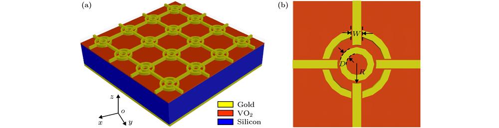
Fig. 1. Adjustable terahertz absorber with multiple defects: (a) Three-dimensional of unit structure; (b) top view of unit structure.多缺陷组合结构可调太赫兹吸收器 (a) 单元结构三维立体图; (b) 单元俯视图
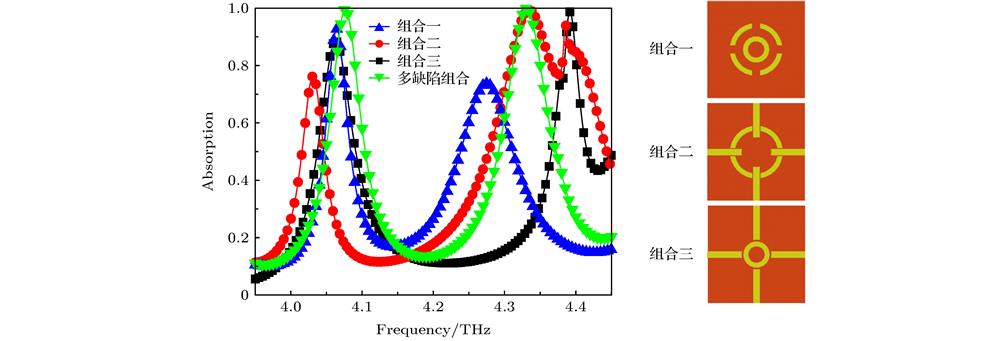
Fig. 2. Absorption curves of the absorber formed by different combinations.不同组合形成的吸收器吸收曲线
Fig. 3. Electric field distribution in TE mode: (a) Combination 1, f = 4.06 THz; (d) combination 2, f = 4.27 THz; (b) combination 2, f = 4.03 THz; (e) combination 2, f = 4.33 THz; (c) combination 3, f = 4.06 THz; (f) combination 3, f = 4.39 THz.
TE模式下电场E 分布图 (a) 组合一, f = 4.06 THz; (d) 组合一, f = 4.27 THz; (b) 组合二, f = 4.03 THz; (e) 组合二, f = 4.33 THz; (c) 组合三, f = 4.06 THz; (f) 组合三, f = 4.39 THz
Fig. 4. Electric field and current distribution in TE mode with multiple defects: (a) f = 4.08 THz, electric field distribution; (b) f = 4.33 THz, electric field distribution; (c) f = 4.08 THz, current distribution; (d) f = 4.33 THz, current distribution.
多缺陷组合TE模式下电场E 和电流A 分布图 (a) f = 4.08 THz, 电场分布; (b) f = 4.33 THz, 电场分布; (c) f = 4.08 THz, 电流分布; (d) f = 4.33 THz, 电流分布
Fig. 5. Absorption curves corresponding to the change of structural parameters: (a) Defect cross distance from center R ; (b) defect ring width W ; (c) center ring width D .
结构参数改变对应的吸收率曲线 (a) 缺陷十字架距离中心距离R ; (b) 缺陷圆环缺陷宽度W ; (c) 中心圆环宽度D
Fig. 6. Changes of VO2 conductivity with temperature.
VO2的电导率随温度的变化
Fig. 7. (a) Absorption of the absorber at different tempera-tures; (b) normalized surface impedance of the absorber.(a) 不同温度下吸收器的吸收率; (b) 吸收器的归一化表面阻抗
Fig. 8. Terahertz absorption spectrum: (a) TE mode; (b) TM mode.太赫兹吸收谱 (a) TE模式; (b) TM模式

Set citation alerts for the article
Please enter your email address
© Copyright 2018-2021 | Chinese Laser Press. All Rights Reserved 沪ICP备15018463号-20