• Acta Physica Sinica
  • Vol. 69, Issue 16, 162901-1 (2020)
Xun Wang*, Feng-Qi Zhang, Wei Chen, Xiao-Qiang Guo, Li-Li Ding, and Yin-Hong Luo
Author Affiliations
  • State Key Laboratory of Intense Pulsed Radiation Simulation and Effect, Northwest Institute of Nuclear Technology, Xi’an 710024, China
  • show less
    DOI: 10.7498/aps.69.20200265 Cite this Article
    Xun Wang, Feng-Qi Zhang, Wei Chen, Xiao-Qiang Guo, Li-Li Ding, Yin-Hong Luo. Experimental study on neutron single event effects of commercial SRAMs based on CSNS[J]. Acta Physica Sinica, 2020, 69(16): 162901-1 Copy Citation Text show less
    Layout of back-n at CSNS[19].
    Fig. 1. Layout of back-n at CSNS[19].
    Comparison between the differential neutron energy spectra of CSNS back-n and Yangbajing.
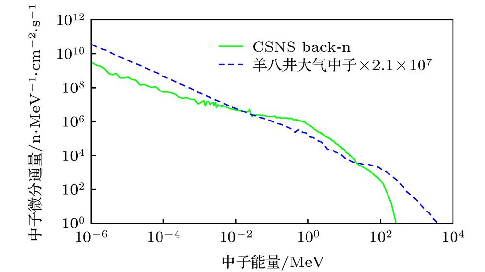
    Fig. 2. Comparison between the differential neutron energy spectra of CSNS back-n and Yangbajing.
    Layout of the irradiation experiment at CSNS back-n
    Fig. 3. Layout of the irradiation experiment at CSNS back-n
    Comparison between the SEE cross sections of devices with different test patterns.
    Fig. 4. Comparison between the SEE cross sections of devices with different test patterns.
    Comparison of the SEE cross sections of the devices with the same feature sizes from different manufacturer: (a) 350 nm SRAM; (b) 130 nm SRAM; (c) 65 nm SRAM.
    Fig. 5. Comparison of the SEE cross sections of the devices with the same feature sizes from different manufacturer: (a) 350 nm SRAM; (b) 130 nm SRAM; (c) 65 nm SRAM.
    Comparison of the SEE cross sections of devices from the same manufacturer with different feature sizes: (a) HITECHI/RENESAS HM SRAM; (b) Cypress CY1318SRAM; (c) Cypress CY62126SRAM; (d) ISSI IS6X SRAM
    Fig. 6. Comparison of the SEE cross sections of devices from the same manufacturer with different feature sizes: (a) HITECHI/RENESAS HM SRAM; (b) Cypress CY1318SRAM; (c) Cypress CY62126SRAM; (d) ISSI IS6X SRAM
    MCU rates of the devices with different test patterns: (a) IS61WV204816(40 nm); (b) CY62126DV(130 nm); (c) HM62V8100 (180 nm); (d) IS64WV25616 (65 nm)
    Fig. 7. MCU rates of the devices with different test patterns: (a) IS61WV204816(40 nm); (b) CY62126DV(130 nm); (c) HM62V8100 (180 nm); (d) IS64WV25616 (65 nm)
    MCU rates and sizes of the devices with the same feature sizes from different manufacturer.
    Fig. 8. MCU rates and sizes of the devices with the same feature sizes from different manufacturer.
    MCU rates and sizes of the devices from the same manufacturer with different feature sizes: (a) CY7C1318; (b) IS6X
    Fig. 9. MCU rates and sizes of the devices from the same manufacturer with different feature sizes: (a) CY7C1318; (b) IS6X
    型号制造商容量/bits特征尺寸/nm工作电压/V
    HM628512AHITACHI4 M (512 K × 8)5005
    HM628512BHITACHI4 M (512 K × 8)3503.3
    HM62V8100RENESAS8 M (1 M × 8)1803.3
    IS62WV1288ISSI1 M (128 K × 8)1303.3
    IS64WV25616ISSI4 M (256 K × 16)653.3
    IS61WV204816ISSI32 M (2 M × 16)403.3
    CY62126VCypress1 M (64 K × 16)3503.0
    CY62126BVCypress1 M (64 K × 16)2503.0
    CY62126DVCypress1 M (64 K × 16)1303.0
    CY7C1318AV18Cypress18 M (1 M × 18)1501.8
    CY7C1318BV18Cypress18 M (1 M × 18)901.8
    CY7C1318KV18Cypress18 M (1 M × 18)651.8
    M328C国产256 K (32 K × 8)651.8
    Table 1.

    Parameters of the SRAM devices for test.

    待测SRAM器件参数

    型号特征尺寸/nm测试图形容量/Mbit注量(>10 MeV)/108n·cm–2翻转数/#翻转截面/10-14cm2·bit–1不确定度/%
    HM628512A5000x00H125.541762.5212.88
    0x55H127.212622.8912.13
    0xAAH125.382153.1812.47
    0xFFH125.362053.0412.56
    HM628512B3500x00H125.712072.8812.54
    0x55H87.031973.3412.64
    0xAAH128.973032.6911.92
    0xFFH123.261142.7814.03
    HM62V81001800x00H245.313432.5711.75
    0x55H245.293672.7611.67
    0xAAH245.293872.9111.61
    0xFFH245.363422.5311.76
    IS62WV12881300x00H19.52555.5117.05
    0xAAH38.051164.5813.97
    0xFFH310.201514.6813.24
    IS64WV25616650x00H84.762716.7912.08
    0x55H84.763398.4911.77
    0xAAH85.233818.6811.63
    0xFFH84.502757.2812.06
    IS61WV204816400x00H644.765341.6711.30
    0x55H644.765231.6411.32
    0xAAH644.765891.8411.22
    0xFFH646.357071.6611.10
    CY62126V3500x55H39.88642.0616.29
    0xAAH39.88712.2815.81
    CY62126BV2500x55H3128.005161.2811.33
    CY62126DV1300x00H310.401153.5314.00
    0x55H310.601394.1613.45
    0xAAH310.401414.3013.41
    0xFFH39.041063.7314.26
    CY7C1318AV181500X55H325.1212937.5210.80
    CY7C1318BV18900X55H324.693812.4211.63
    CY7C1318KV18650X55H325.093742.1911.65
    M328C650X55H0.751161671.8413.00
    Table 2.

    Test results of the SEUs at CSNS back-n.

    在CSNS反角白光中子源的SEU测试结果

    型号特征尺寸/nm不同测试图形时MCU占比最大MCU位数
    0x000x55H0xAAH0xFFH
    HM628512A50000001
    HM628512B35000001
    HM62V81001802.33%5.94%1.09%4.68%2
    IS62WV128813004.65%02
    IS64WV25616659.59%9.14%6.01%0.73%3
    IS61WV2048164028.29%24.09%28.52%25.00%7
    CY62126V35000001
    CY62126BV25000001
    CY62126DV13040.00%35.97%35.46%45.28%3
    CY7C1318AV1815036.13%4
    CY7C1318BV189042.31%6
    CY7C1318KV186556.80%7
    M328C6514.37%2
    Table 3.

    Extraction results of the single event multiple cell upsets.

    单粒子MCU提取结果

    Xun Wang, Feng-Qi Zhang, Wei Chen, Xiao-Qiang Guo, Li-Li Ding, Yin-Hong Luo. Experimental study on neutron single event effects of commercial SRAMs based on CSNS[J]. Acta Physica Sinica, 2020, 69(16): 162901-1
    Download Citation