
Chenyang Yue, Hong Jiang, Tianzhi Li, Siyan Yao, Shengyue Zeng, Xiaojun Xu, Chaofan Zhang, "Compact in situ microscope for photoelectron spectroscopy via two-mirror reflection," Chin. Opt. Lett. 21, 061101 (2023)
- Chinese Optics Letters
- Vol. 21, Issue 6, 061101 (2023)
Abstract
Keywords
1. Introduction
Photoelectron spectroscopy is a powerful tool in direct investigation of the electronic structure of materials. The requirement of photoelectron spectroscopy with spatial resolution has become urgent both in scientific research and industry applications[1–7]. However, the processes of scanning the whole sample and especially targeting the specific region of interest are usually very time-consuming. An assisting in situ microscope could significantly improve probing efficiency. Similar inconvenience also exists in other types of electronic microscopes, including the scanning electron microscope (SEM)[8], the transmission electron microscope (TEM)[9–11], the scanning tunneling microscope (STM)[12], tip-enhanced Raman spectroscopy (TERS)[13], and photoemission electronic microscopy (PEEM)[14]. Several methods have been tried to solve this problem. As for the spatial and angular-resolved photoemission spectroscopy (sr-ARPES), by now only one system (the end station at the Elettra synchrotron in Italy)[15–17] with an assisting optical microscope has been reported, utilizing a homemade miniature photoelectron analyzer and telescopic optical structure, the configuration of which makes the direct view of microscopy possible. Unfortunately, it is not real in situ but side assisting. In the other setups of electronic microscopy, the most common method currently used is to have a conventional microscope adhere the windows of the experimental vacuum chamber. This poses some obstacles to the operation and causes a limitation of magnification. To the best of our knowledge, the scheme of an in situ microscope simultaneously implementing photoelectron spectroscopy is still lacking.
The design and realization of the in situ optical microscope for photoelectron spectroscopy may face many difficulties. First, to realize in situ monitoring of samples, the components of the optical microscope need to keep away from the head of the photoelectron analyzer that directly faces the sample surface, with only few centimeters in between. Second, since the direct microscope on top is not possible, the new configuration design should naturally consider the idea of bending the optical path, due to the limited space in an ultrahigh vacuum (UHV) chamber. The objective lenses have to be mounted away from the sample area, which results in a distance of at least 100 mm from the sample to the objective lens, making the realization of high resolution and large magnification difficult.
In this paper, we report a compact in situ microscope for photoelectron spectroscopy as a side-assisting optical system inside a UHV chamber. The microscope is designed with a macro lens instead of an objective lens, achieving the best spatial resolution and 1:1 magnification at a long objective distance of 200 mm. Two-mirror reflection is employed to guide the optical path from the sample surface to the macro lens. In this configuration, there is no optical component mounted directly over the surface of the sample, thus avoiding the blocking of the emitting photoelectrons of the sample to the electronic energy analyzer. A microscope is installed downstream from the optical path to achieve a large magnification. Combined with the microscopic lens group and macro lens, the total optical magnification of
Sign up for Chinese Optics Letters TOC. Get the latest issue of Chinese Optics Letters delivered right to you!Sign up now
2. Methods
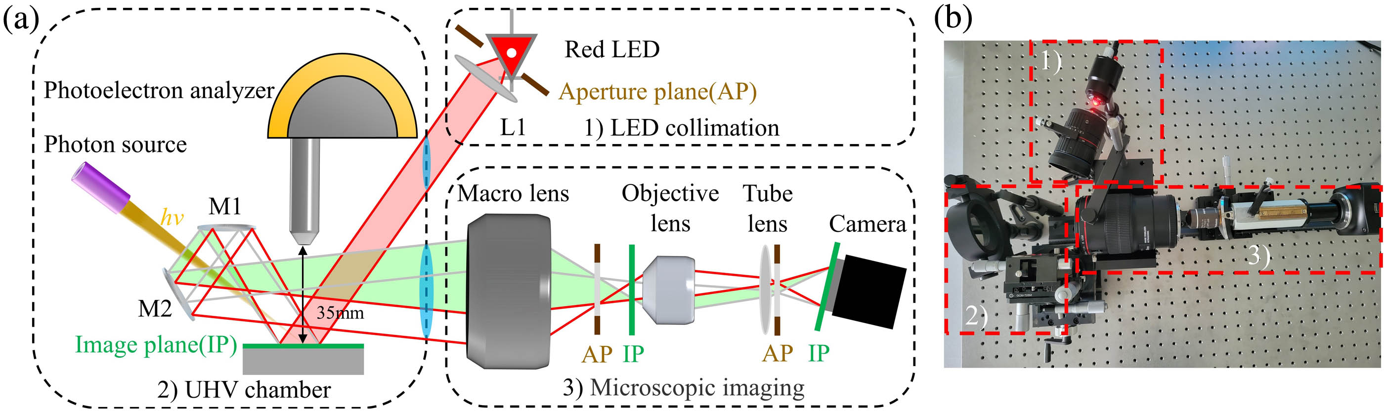
Figure 1 illustrates the schematic drawing of the system we propose, which contains three functional parts: an LED collimation stage, an ultrahigh vacuum chamber, and a microscopic imaging part. The observation path and the sample are placed in parallel. In this way, other detectors or probing means can be applied directly above the sample.
![]()
Figure 1.Principle and scheme of the side-assisting microscope. (a) Principal optical setup including three parts: (1) LED collimation stage; (2) ultrahigh vacuum chamber; (3) microscopic imaging. (b) Photo of the experimental setup in a clean laboratory air environment.
As the standard UHV testing chamber shows, a photoelectron analyzer is placed directly above the sample, and the distance from its extreme end to the specimen is only 35 mm. This avoids the microscope blocking the photoelectron collection of the analyzer and setting the reflected light receiving configuration away from the main photon-in-electron-out path is necessary. In addition, considering the very limited space in a vacuum chamber, we only set two mirrors to transmit the reflected light out of the sample-analyzer area. The illumination light, mounted outside the UHV, with a center wavelength of 620 nm from a red LED (Daheng Optics, GCI-060401) is first collimated by a lens L1 (Foctek Photonics, C-M35-1F12) to form a virtually 0.5-mm-diameter wide beam. After passing through the vacuum window, the light source is defocused onto the specimen. The beam is reflected off the sample, consequently passes through two mirrors, M1 and M2, and then goes into microscopic imaging part, which is fixed on a five-axis motorized stage. Subsequently, the reflected light passes through a macro lens that is set to converge the light and compensate for tilt error. The obtained image plane (IP) is located at the front focal plane of the objective lens (Olympus). Combined with tube lens (Olympus, SWTLU-C) to realize infinite observation, the objective lens can be replaced with a different numerical aperture (NA) to achieve various magnification. The tube lens finally forms the image on the sensor of a low-noise and high dynamic range CMOS camera (Phenix, MC-DK20U(C)-TP).
In order to ensure that the microscopic imaging part is sitting away from the electronic analyzer, a long object distance of at least 200 mm is required. However, the object distances of traditional telephoto lenses are generally less than 100 mm, which limits the choice of objective lens with large NA. We therefore use a macro lens (Canon, EF 100 mm f/2.8 IS USM) as a special kind of imaging lens, which not only meets the demand of object distance, but can achieve the 1× magnification at the closest focusing distance of 300 mm (the minimum magnification is 0.5×). Equipped with different objective lenses (
3. Experimental Results
To evaluate the imaging quality of our compact in situ optical microscope, a combined test target (Lbtek, RTR1Ee) suitable for multiple tests with a United States Air Force (USAF) resolution test target (six groups with six element sizes), a grid pattern of 100 µm, and a group of variable line gratings (1.25 lp/mm to 250 lp/mm) were used. In this experiment, the objective lens with magnification of
![]()
Figure 2.System spatial resolution testing. (a) Image of a USAF target (groups 6 and 7); (b) region for experimenting; (c) and (d) assessed resolution of the side-assisting microscope system along the solid line (X and Y) of (b), respectively.
To characterize the possible field curvature of the system, we next selected vertically oriented grating (50 lp/mm) with a 10 µm step size. The result is shown in Fig. 3(a), where the microscopic image is provided in the insets as references. From the image in Fig. 3(a), a line cut of intensity distribution across the lines is taken and shown in Fig. 3(b), clearly showing the expected period of 20 µm. Then, the derivative of the line cut intensity with respect to longitudinal position is used to measure the difference of resolution between the central and fringe FOVs. As the derivative (red line) in Fig. 3(b) shows, each peak represents the LSF of the upper edge of a bright stripe, whereas each trough represents the LSF of the bottom edge, resulting in the different FWHM shown in Fig. 3(c). It is obvious that the FWHM of the wave peak is generally larger than the corresponding trough, which means the resolution of the bottom edge is better than that of the upper edge. We attempted to interpret this phenomenon. The combined resolution plate has a certain thickness and only the test pattern is coated with Cr, which causes the illumination light to pass through in the remaining positions. Since our system uses sideways illumination, the light may be reflected many times in the backward direction of the target and transmitted from one side, resulting in a false image on that side and thus reducing the resolution. In addition, it can be clearly seen that the FWHM at the middle of the image is significantly lower than that at the edge. The maximum difference is only 0.5 µm, indicating that the resolution of the center is slightly better than that of the edge, both in upper and bottom areas. The result shows that a certain field curvature exists in the system, leading to the decrease in resolution in the edge position. However, the resolution reduction of 0.5 µm has little effect on the side-assisting observation of wide FOV in photoelectron spectroscopy, which benefits from the correction of the Scheimpflug principle, confirming our microscope can well provide in situ optical observation.
![]()
Figure 3.System field curvature testing. (a) Two-dimensional image of a 20 µm-period grating with a vertical orientation. The inset in (a) shows a microscopic image of the grating. (b) The intensity profile (blue line) extracted along the white solid line in (a) and the first derivative of the line cut (red line); (c) FWHM corresponding to the peaks (black line) and troughs (red line) of the first derivatives of the intensity in (b).
Considering that the purpose of our system is to assist the photoelectron spectroscopy to probe the whole area of interest, the image field distortion of the microscope is required to be controlled to a small level to ensure the accuracy of localization. To quantify the degree of distortion, a standard grid pattern of 100 µm [Fig. 4(a)] was placed within the view. The result is shown in Fig. 4(b), which includes 16 complete grid patterns. Using the standard grid in Fig. 4(a) as a reference, the intensity curves are plotted in Figs. 4(c) and 4(d) along the horizontal and vertical yellow solid lines in Fig. 4(a), respectively. The same approach is applied to the resulting intensity curves. In comparison with the intensity profiles of the standard grid and the result, it is observed that the peak positions of both are almost identical. Since our work is concerned with the relative position of the feature in the sample and the aberration only changes the position of the off-axis object point on the ideal surface, no distortion can be observed in the two axes orthogonal to each other at the center in Fig. 4(b). Thus, the distortion can be defined as
![]()
Figure 4.System distortion testing. (a) Standard grid pattern of 100 µm; (b) experimental result of standard grid pattern; (c) intensity profiles of standard grid (black lines) and experimental result (red lines) plotted via the horizontal yellow solid lines in (a) and (b); (d) intensity profiles of standard grid and experimental result plotted via the vertical yellow solid lines in (a) and (b); insets in (c) and (d) show the distortion of X direction and Y direction, respectively.
To further validate the imaging feasibility of the system in actual material sample, a device was prepared with a specific gold electrode pattern of parallel microline structures. The image of the device is provided in Fig. 5(a) as a reference; it has an overall size of
![]()
Figure 5.Experimental results and quantitative analysis. (a) Sample morphology and region for experimenting; (b) result of square-shaped area; (c) and (d) resolution measured along the two line cuts in (b), respectively; (e) result of central stripe area with our setup; (f) result of conventional high-resolution optical microscope at 40×.
First, the optical resolution of our setup in the material sample experiment is evaluated by plotting the intensity profiles via the line cuts obtained from Fig. 5(d), both in the directions of X and Y. As can be expected, the space limitation directly above the sample causes the illumination light to be obliquely incident, making a lower vertical resolution rather than a horizontal; a similar phenomenon can be seen in the testing of combined targets. Indeed, as shown in Figs. 5(e) and 5(f), the resolution measured along the two axes is slightly different, being 4.08 µm along the direction perpendicular to the incident plane, and 4.49 µm along the direction parallel to it. It is noteworthy that the resolution measured in the sample experiment was improved by about 2 µm, compared to the result of the resolution plate. This may be due to the tiny thickness of the material sample, resulting in little effect on the reflected light from the bottom, the condition readily available in photoelectron spectroscopy and other electronic microscopes (the thickness is typical only in the hundred nanometer range).
As Fig. 5(e) demonstrates, the stripes with 10 µm interval can be clearly distinguished by the system and no obvious field curvature or distortion exists at the edge of the FOV. Furthermore, in comparison with the result of the same area under conventional optical microscope at
![]()
Figure 6.Microscope images of graphene flake. (a) Conventional optical microscope image of the sample at 25×; (b) microscope image with the proposed setup.
4. Conclusion
In summary, we have designed and built a compact in situ microscope for photoelectron spectroscopy, solving the problem of the inconformity for mounting an in situ microscope and the difficulty of samples to zoom in with a large magnification. The observation path of our microscope in this paper and the sample in UHV are placed in parallel, avoiding obstructing other detectors from observing directly over the sample. We used the macro lens to replace the objective lens in the conventional optical microscope, achieving a 1:1 magnification at a long object distance of 200 mm. Combined with the microscope lens group, we achieved a maximum magnification of 100 times. The long object distance can satisfy the configuration of most photoelectron spectroscopy and other electronic microscopies, making the microscopic imaging part of our system mounted away from the main probing means. Even though a few setups may require a longer object distance, it can be achieved by adjusting the macro lens, though it will lose some resolution and magnification. According to the experimental results, the lateral resolution can reach 4.08 µm, and the longitudinal resolution can achieve 4.49 µm. The impact of curvature only makes a 0.5 µm resolution reduction in the edge, and distortion could be controlled to a small level, to less than
References
[8] J. Zach, M. Haider. Correction of spherical and chromatic aberration in a low voltage SEM. Optik, 98, 112(1995).
[11] A. H. Zewail. Four-dimensional electron microscopy. Science, 328, 187(2010).
[12] S. Park, C. F. Quate. Scanning tunneling microscope. Rev. Sci. Instrum., 58, 2010(1987).
[13] V. Deckert. Tip-enhanced Raman spectroscopy. J. Raman Spectrosc., 40, 1336(2010).
[18] M. Corbett, N. Maycock, E. Rosen, D. O’Brart. Scheimpflug camera-based systems. Corneal Topography: Principles and Applications, 43(2019).


Set citation alerts for the article
Please enter your email address

© Copyright 2018-2021 | Chinese Laser Press. All Rights Reserved 沪ICP备15018463号-20