• Chinese Physics B
  • Vol. 29, Issue 9, (2020)
Bin Guo1, Kai-Ge Shi1, Hai-Lang Qin1, Liang Zhou1, Wei-Qiang Chen1, Fei Ye1, Jia-Wei Mei1, Hong-Tao He1, Tian-Luo Pan1、†, and Gan Wang1、2
Author Affiliations
  • 1Shenzhen Institute for Quantum Science and Engineering & Department of Physics, Southern University of Science and Technology, Shenzhen 58055, China
  • 2Guangdong Provincial Key Laboratory of Quantum Science and Engineering, Shenzhen Institute for Quantum Science and Engineering, Southern University of Science and Technology, Shenzhen 518055, China
  • show less
    DOI: 10.1088/1674-1056/abaf9c Cite this Article
    Bin Guo, Kai-Ge Shi, Hai-Lang Qin, Liang Zhou, Wei-Qiang Chen, Fei Ye, Jia-Wei Mei, Hong-Tao He, Tian-Luo Pan, Gan Wang. Evidence for topological superconductivity: Topological edge states in Bi2Te3/FeTe heterostructure[J]. Chinese Physics B, 2020, 29(9): Copy Citation Text show less
    MBE growth of the Bi2Te3 and FeTe films. (a) The schematic crystal structure of Bi2Te3 and FeTe. (b) The RHEED pattern of the STO surface which shows that the substrate has a well-defined 2 × 1 surface reconstruction. (c) The RHEED pattern of the FeTe surface. (d) The RHEED pattern of the Bi2Te3 surface. The double-line structure shows two kinds of domains in the Bi2Te3 film. (e) Schematic of two types of Bi2Te3 crystal domains on FeTe.
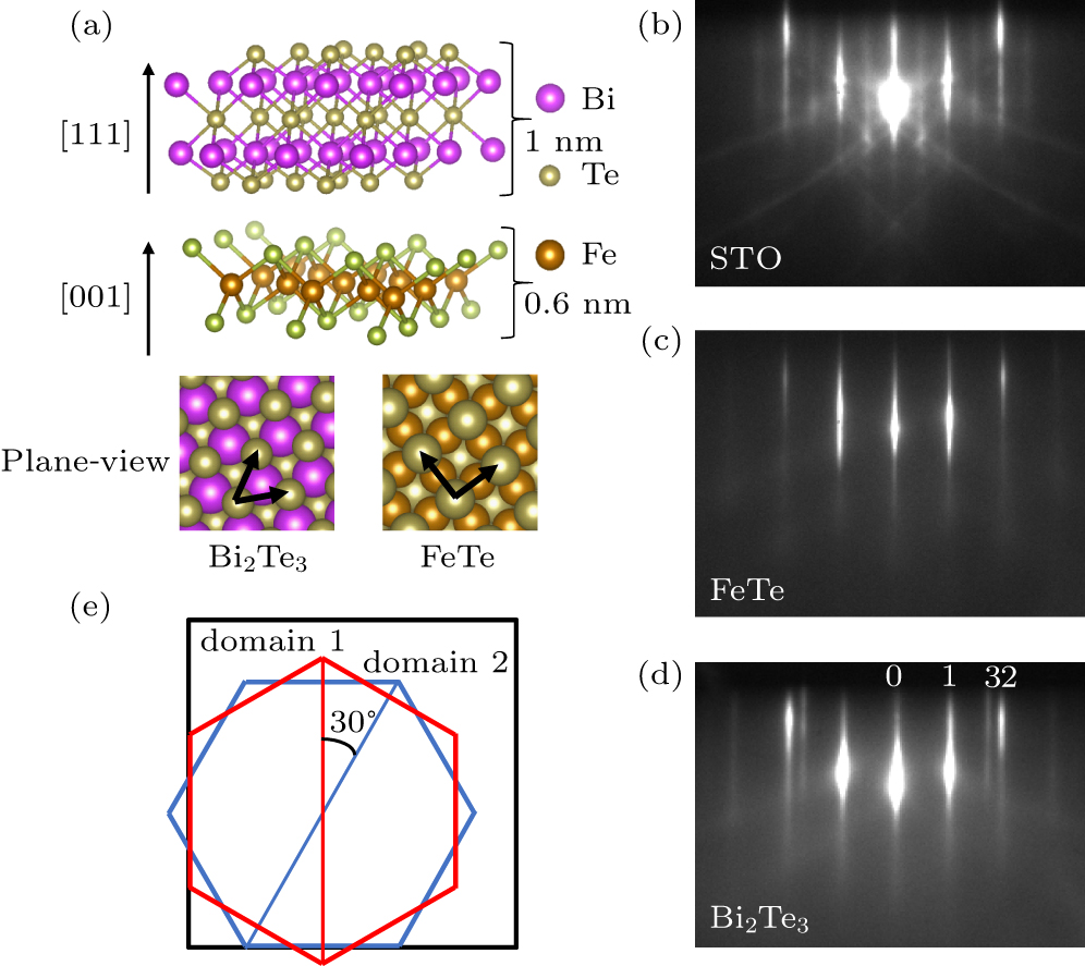
    Fig. 1. MBE growth of the Bi2Te3 and FeTe films. (a) The schematic crystal structure of Bi2Te3 and FeTe. (b) The RHEED pattern of the STO surface which shows that the substrate has a well-defined 2 × 1 surface reconstruction. (c) The RHEED pattern of the FeTe surface. (d) The RHEED pattern of the Bi2Te3 surface. The double-line structure shows two kinds of domains in the Bi2Te3 film. (e) Schematic of two types of Bi2Te3 crystal domains on FeTe.
    (a), (b) Photoemission intensity of the cut along the Γ–M direction of FeTe acquired on pure FeTe and 0.5 QL Bi2Te3/FeTe heterostructure, respectively. (c) Plot of EDCs of (b). (d), (e) Differential intensity maps of (a) and (b). (f) Photoemission intensity of the cut along the Γ–K direction of Bi2Te3 on 2 QLs Bi2Te3/FeTe sample.
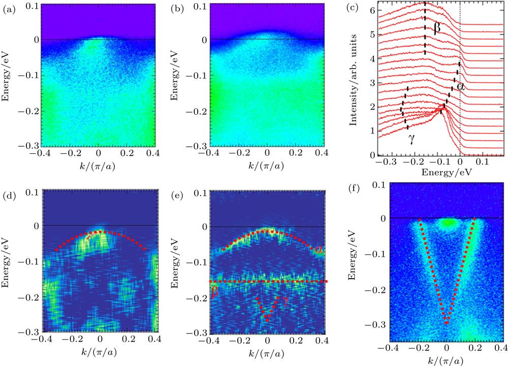
    Fig. 2. (a), (b) Photoemission intensity of the cut along the ΓM direction of FeTe acquired on pure FeTe and 0.5 QL Bi2Te3/FeTe heterostructure, respectively. (c) Plot of EDCs of (b). (d), (e) Differential intensity maps of (a) and (b). (f) Photoemission intensity of the cut along the ΓK direction of Bi2Te3 on 2 QLs Bi2Te3/FeTe sample.
    (a) An STM image of different sizes of 1 QL Bi2Te3 islands on the FeTe terrace. (150 × 150 nm2, VBias = 200 mV, ITunnel = 50 pA). (b) STS curves taken over different positions on different size Bi2Te3 islands with Roman numbers indicating their positions (set point: VBias = 200 mV, ITunnel = 50 pA, modulation voltage: ΔV = 300 μV). (c) Zoom in image of an island in (a). (20 × 20 nm2, VBias = 200 mV, ITunnel = 50 pA). (d) STS curves acquired over position IV in (c) under different tip states (set point: VBias = 200 mV, ITunnel = 50 pA, modulation voltage: ΔV = 300 μV).
    Fig. 3. (a) An STM image of different sizes of 1 QL Bi2Te3 islands on the FeTe terrace. (150 × 150 nm2, VBias = 200 mV, ITunnel = 50 pA). (b) STS curves taken over different positions on different size Bi2Te3 islands with Roman numbers indicating their positions (set point: VBias = 200 mV, ITunnel = 50 pA, modulation voltage: ΔV = 300 μV). (c) Zoom in image of an island in (a). (20 × 20 nm2, VBias = 200 mV, ITunnel = 50 pA). (d) STS curves acquired over position IV in (c) under different tip states (set point: VBias = 200 mV, ITunnel = 50 pA, modulation voltage: ΔV = 300 μV).
    (a) A zoom in STM image showing the edge of a 1 QL Bi2Te3 island (32 × 32 nm2, VBias = 2.5 mV, ITunnel = 50 pA). (b)–(d) dI/dV mappings over (a) at 0.5 mV, –0.5 mV, and 1.5 mV, respectively (32 × 32 nm2, set points: VBias = 2.5 mV, ITunnel = 50 pA, modulation voltage: ΔV = 300 μV).
    Fig. 4. (a) A zoom in STM image showing the edge of a 1 QL Bi2Te3 island (32 × 32 nm2, VBias = 2.5 mV, ITunnel = 50 pA). (b)–(d) dI/dV mappings over (a) at 0.5 mV, –0.5 mV, and 1.5 mV, respectively (32 × 32 nm2, set points: VBias = 2.5 mV, ITunnel = 50 pA, modulation voltage: ΔV = 300 μV).
    (a) Zoom in atomic resolution STM images showing the top edge of the Bi2Te3 island in Fig. 4(a) between the Bi2Te3 island (bottom) and the FeTe terrace (top), respectively. Red points with numbers indicate positions where STS curves were taken (15 × 15 nm2, VBias = 10 mV, ITunnel = 1.5 nA). (b) and (c) STS curves taken on the labeled positions in (a) on the FeTe terrace and the Bi2Te3 island (set points: VBias = 10 mV, ITunnel = 1.5 nA, modulation voltage: ΔV = 300 μV). All spectra are offset vertically for clarity with dotted lines indicating the 0 position before the offset. (d) ZBC of the spectrum in (b) and (c) vs. distance from the edge. Blue line indicates the edge position. Red numbers indicate spectra positions. Dashed lines below each spectrum indicate the respective zero dI/dV value. (e) STS spectra Nos. 4–6, taken on the Bi2Te3 island in (c) after the subtraction of the most inner No. 1 spectrum.
    Fig. 5. (a) Zoom in atomic resolution STM images showing the top edge of the Bi2Te3 island in Fig. 4(a) between the Bi2Te3 island (bottom) and the FeTe terrace (top), respectively. Red points with numbers indicate positions where STS curves were taken (15 × 15 nm2, VBias = 10 mV, ITunnel = 1.5 nA). (b) and (c) STS curves taken on the labeled positions in (a) on the FeTe terrace and the Bi2Te3 island (set points: VBias = 10 mV, ITunnel = 1.5 nA, modulation voltage: ΔV = 300 μV). All spectra are offset vertically for clarity with dotted lines indicating the 0 position before the offset. (d) ZBC of the spectrum in (b) and (c) vs. distance from the edge. Blue line indicates the edge position. Red numbers indicate spectra positions. Dashed lines below each spectrum indicate the respective zero dI/dV value. (e) STS spectra Nos. 4–6, taken on the Bi2Te3 island in (c) after the subtraction of the most inner No. 1 spectrum.
    Bin Guo, Kai-Ge Shi, Hai-Lang Qin, Liang Zhou, Wei-Qiang Chen, Fei Ye, Jia-Wei Mei, Hong-Tao He, Tian-Luo Pan, Gan Wang. Evidence for topological superconductivity: Topological edge states in Bi2Te3/FeTe heterostructure[J]. Chinese Physics B, 2020, 29(9):
    Download Citation