Shaolong Yan, Jianliang Huang, Ting Xue, Yanhua Zhang, Wenquan Ma. Long wavelength interband cascade photodetector with type II InAs/GaSb superlattice absorber[J]. Journal of Semiconductors, 2023, 44(4): 042301
Copy Citation Text
We report on a long wavelength interband cascade photodetector with type II InAs/GaSb superlattice absorber. The device is a three-stage interband cascade structure. At 77 K, the 50% cutoff wavelength of the detector is 8.48 μm and the peak photoresponse wavelength is 7.78 μm. The peak responsivity is 0.93 A/W and the detectivity D* is 1.12 × 1011 cm·Hz0.5/W for 7.78 μm at –0.20 V. The detector can operate up to about 260 K. At 260 K, the 50% cutoff wavelength is 11.52 μm, the peak responsivity is 0.78 A/W and the D* is 5.02 × 108 cm·Hz0.5/W for the peak wavelength of 10.39 μm at –2.75 V. The dark current of the device is dominated by the diffusion current under both a small bias voltage of –0.2 V and a large one of –2.75 V for the temperature range of 120 to 260 K.We report on a long wavelength interband cascade photodetector with type II InAs/GaSb superlattice absorber. The device is a three-stage interband cascade structure. At 77 K, the 50% cutoff wavelength of the detector is 8.48 μm and the peak photoresponse wavelength is 7.78 μm. The peak responsivity is 0.93 A/W and the detectivity D* is 1.12 × 1011 cm·Hz0.5/W for 7.78 μm at –0.20 V. The detector can operate up to about 260 K. At 260 K, the 50% cutoff wavelength is 11.52 μm, the peak responsivity is 0.78 A/W and the D* is 5.02 × 108 cm·Hz0.5/W for the peak wavelength of 10.39 μm at –2.75 V. The dark current of the device is dominated by the diffusion current under both a small bias voltage of –0.2 V and a large one of –2.75 V for the temperature range of 120 to 260 K.
Introduction
Long wavelength (LW) infrared photodetectors have important applications in military and civil sectors. Compared to HgCdTe, InAs/GaSb type II superlattice (T2SL) material may have some advantages for the LW infrared range in terms of low cost and high uniformity[1-3]. However, at high temperature, the short diffusion length and the high dark current limit the detector's performance. Several barrier detector structures have been proposed to lower the dark current of the T2SL detector[4-9]. Originating from the interband cascade laser structure[10], the interband cascade infrared photodetectors (ICIPs) based on T2SL materials have also attracted interest[11-15] and have demonstrated some enhanced performance, especially at high temperature[16] and high-speed operation[17-19]. The T2SL ICIP is usually comprised of a multiple series of connected cascade stages. Each stage has a T2SL absorber sandwiched by an electron barrier (EB) and a hole barrier (HB). The merit of using the multiple-stage design is that it can avoid the limit of the short diffusion length at high temperature. In this design, for each stage, the absorber layer is thinner than the diffusion length to guarantee the total transport of the photogenerated carriers. In addition, a multiple-stage structure can further increase the total series resistance of the device and can correspondingly reduce the dark current. Based on these features, the T2SL ICIP may have some advantages for high temperature operation for the LW detection.
In this paper, we report on a LW infrared photodetector with a three-stage interband cascade structure using InAs/GaSb T2SL materials as the absorber. At 77 K, the 50 % cutoff wavelength of the ICIP detector is 8.48 μm and the peak response wavelength is 7.78 μm. The peak responsivity is 0.93 A/W and the detectivity D* is 1.12 × 1011 cm·Hz0.5/W at the peak response wavelength at –0.20 V.
At 260 K, the 50% cutoff wavelength is 11.52 μm and the D* is 5.02 × 108 cm·Hz0.5/W at the peak response wavelength of 10.39 μm with the peak responsivity of 0.78 A/W. The dark current of the device is dominated by the diffusion current under both a small and a large bias when the temperature is from 120 to 260 K.
Design and growth
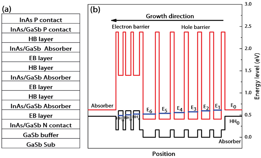
Fig. 1(a) is a schematic drawing of the ICIP epitaxy structure andFig. 1(b) shows the band diagram of the structure of one stage. The ICIP device consists of an n contact layer, a three-stage interband cascade structure, and a p contact layer. The n contact layer is made up of a 0.5 μm thick GaSb layer doped to 2 × 1018 cm−3 using GaTe and 0.5 μm thick InAs(24 Å)/GaSb(24 Å) SLs with the InAs layer doped to 2 × 1018 cm−3. The p contact layer is comprised of 0.3 μm thick InAs(24 Å)/GaSb(24 Å) SLs with the GaSb layer doped to 2 × 1018 cm−3 followed by 200 Å thick InAs layer doped to 2 × 1018 cm−3 using Be. For the three-stage interband cascade structure, each stage has a T2SL absorber sandwiched by an EB and an HB. The absorber layer of each stage is InAs (39 Å)/GaSb(26 Å) SLs with different thickness. Specifically, from the top to the bottom, the absorber layer is 600, 740, and 900 nm thick for the three stages, respectively. All three absorber layers are lightly doped using Be (1 × 1016 cm−3). For the barrier layers, we base our design on Ref. [12] and make some changes in terms of the thickness and the number of quantum wells. The specific barrier structure of our ICIP is designed by using the 8-band k·p model calculation. The specific HB layer is made up of quantum wells in alternate AlSb/InAs order of 21/72/22/65/23/59/24/54/23/48/21/45/21, in unit of Å. According to our calculation, the electron states in the HB layer may be regarded as a cascade of nearly equidistributed states in which the energy difference between the adjacent levels is equal to a longitudinal optical phonon energy. Therefore, the photogenerated electrons can be extracted out of the HB layer effectively. The photogenerated electrons in one absorber layer should first pass through the HB layer by the optical phonon-assisted tunneling and then reach to the hole states of the EB layer and finally tunnel to the valence band of the absorber in the next stage. Similarly, the EB layer consists of quantum wells in alternate AlSb/GaSb order of 15/27/15/30/15/35/21, in unit of Å. The energy levels in the valence band of the EB layer are also nearly equidistributed. Thus, this EB layer serves as a function of tunneling layer, allowing the photogenerated electrons tunnel to the next stage through the EB valence band.
Figure 1.(Color online) (a) Schematic drawing of the epitaxy structure of the device. (b) Band structure of the EB and HB parts.
The sample is grown on an n type GaSb (001) substrate by molecular beam epitaxy. High resolution X-ray diffraction (XRD) measurement is performed for the as-grown sample. The full width at half-maximum of the 0-th XRD satellite peak is 38.4 arcsec, revealing a high structural quality. The SL period of the absorber of the sample is determined to be 66.3 Å, which is close to our design. The as-grown sample is then processed into a circular mesa structure by standard photolithography, lift-off, dry and wet etching techniques without any surface passivation. A mixture of citric acid, H3PO4, H2O2 and H2O is employed for 10 s after inductively coupled plasma etching to smooth the surface and to eliminate the etching induced surface damages. Finally, Ti(100 nm)/Au(300 nm) metal films are deposited by electron-beam evaporation for the ohmic contact metallization. The diameter of the circular mesa is 400 μm.
Results and discussion
Fig. 2(a) is the measured dark current density curves of the ICIP device from 77 to 260 K. At 77 K, the dark current density is 6.25 × 10⁻⁴ A/cm2 at –0.20 V and the corresponding product of the dynamic resistance and area (RdA) is 977.27 Ω·cm2. At 260 K, the dark current density is 21.55 A/cm2 and the RdA is 0.13 Ω·cm2 at –2.75 V.Fig. 2(b) shows the dependences of the dark current density on 1000/T when the applied bias voltage is –0.20 and –2.75 V. From this Arrhenius plot, for the temperature range of 120 to 260 K, the activation energy is extracted to be 0.118 and 0.097 eV at –0.20 and –2.75 V, respectively. For a T2SL structure, the 50% cutoff wavelength of the photoresponse practically coincides with the bang gap of the SL absorber, i.e., e1-hh1 transition. Therefore, when the temperature is above 120 K, at –0.2 V, the extracted activation energy is very close to the energy of the 50% cutoff wavelength of the detector response [seeFig. 3(a) below]; at –2.75 V, the activation energy is slightly decreased but still stays nearly close to the energy of the 50% cutoff wavelength. This implies that the dark current of the ICIP detector is dominated by the diffusion mechanism under both a small and a large bias when the temperature is from 120 to 260 K. For the low temperature range of 77 to 120 K, the activation energy is extracted to be only 0.054 and 0.034 eV when the bias voltage is –0.2 and –2.75 V, respectively. Although this shallow activation energy is widely observed for T2SL detectors, its origin is still the subject of debate; for example, it could be due to the background irradiation[20] or other effects[21].
Figure 2.(Color online) (a) The dark current density curves of the device at different temperatures. (b) The Arrhenius plots of the dark current density vs temperature of the device at –0.2 and –2.75 V.
Figure 3.(Color online) (a) The normalized photoresponse spectra of the ICIP device at different temperatures. (b) and (c) are the peak responsivity of the ICIP device vs bias voltage at different temperature ranges.
Fig. 3(a) depicts the normalized photoresponse spectra at different temperatures. The 50% cutoff wavelength is 8.48 μm at 77 K and is 11.52 μm at 260 K. The spectral photoresponse of the device is measured by a Fourier transform infrared spectrometer. The dip in the response spectra is at around 9.6 μm and its wavelength does not change when changing the temperature. We tend to think that the dip might be caused by the absorption of ozone in the air. The blackbody photocurrent is measured with a blackbody temperature set at 800 K. The responsivity of the detector is obtained by calibrating the spectral photoresponse with the blackbody photocurrent.Figs. 3(b) and3(c) show the measured dependence of the responsivity on the applied bias voltage for different temperature ranges. At 77 K, the responsivity maximum of the ICIP is 0.93 A/W at –0.20 V for the peak wavelength of 7.78 μm and the corresponding quantum efficiency (QE) is 14.8%. At 260 K, the responsivity maximum is 0.78 A/W at the peak wavelength of 10.39 μm at –2.75 V and the corresponding QE is 9.3%. It can be seen that there is a "turn-on" voltage at which the responsivity reaches the maximum. This turn-on voltage differs when the temperature is changed. For the temperature range roughly between 77 and 200 K, this turn-on voltage is relatively small and is smaller than 1 V [Fig. 3(b)]. When the temperature is above 200 K, the turn-on voltage is larger than 1 V [Fig. 3(c)]. This difference of the turn-on voltage at different temperatures could be caused by two factors. First, there is a misalignment of the energy levels among the absorber, the EB and the HB layer. An increased electric field through an increased applied bias voltage can change the energy levels and may reduce or even eliminate the misalignment of the energy levels. This is equivalent to the quantum Stark effect. Second, when the temperature is increased, the diffusion length is decreased. It has been reported that the diffusion length for the mid wavelength range at room temperature is about 0.4 μm[22]. Since the diffusion length of a LW device is much shorter than that of a mid wavelength device, the absorber layer thickness in the first stage in our LW device is 0.6 μm. This may imply that the diffusion length is even shorter than the absorber layer thickness. Therefore, the device needs an extra bias to collect more photogenerated carriers and to achieve the responsivity maximum. When the temperature is above about 200 K, the diffusion length probably becomes shorter than the absorber layer in one stage, which makes the turn-on voltage larger as observed. This implies that the second factor predominates the turn-on voltage when the temperature is above 200 K. This also means that there is still room to optimize the device structure to reduce the turn-on voltage and to further enhance the device performance.
The overall device performance can be seen inFig. 4(a), which shows the responsivity, QE, and the detectivity D* at the peak wavelength at different temperatures. Here, the D* of the ICIP device is calculated by
Figure 4.(Color online) (a) The peak responsivity, the QE and the D* of the detector at different temperatures. (b) The D* spectra at four different temperatures.
Here, Rp is the responsivity, e is the electron charge, Jd is the dark current density, RdA is the dynamic resistance-area product, R0A is the dynamic resistance-area product at zero bias, Kb is Boltzmann’s constant and T is temperature. The evaluation of the D* of an ICIP is described in detail in Ref. [23]. Eq. (1) is based on Ref. [23] but the contribution of the dark current induced noise is added to the equation, which is the first term in the square root in the denominator of Eq. (1). The reason is that the dark current induced noise becomes significant for a large bias voltage, such as –2.75 V. As shown inFig. 4(b), the calculated D* is 1.12 × 1011 cm·Hz0.5/W for the peak wavelength of 7.78 μm at 77 K and is 1.42 × 109 cm·Hz0.5/W at 200 K. At 260 K, the maximum D* becomes 5.02 × 108 cm·Hz0.5/W at the peak wavelength of 10.39 μm at –2.75 V. As mentioned earlier, the responsivity reaches 0.78 A/W at –2.75 V at 260 K. Therefore, even at 260 K, this is a reasonable result. This performance of our ICIP is nearly in the neighborhood of that of some reported LW ICIP detectors with close detection wavelength[12].
Conclusion
In summary, we have designed and demonstrated a LW ICIP using InAs/GaSb T2SL material as the absorber. The device is a three-stage interband cascade structure. At 77 K, the 50% cutoff wavelength of the ICIP device is 8.48 μm and the peak photoresponse wavelength is 7.78 μm. The peak responsivity is 0.93 A/W and the D* is 1.12 × 1011 cm·Hz0.5/W for 7.78 μm at –0.20 V. The dark current of the device is dominated by the diffusion current under a small and a large bias for the temperature range of 120 to 260 K. At 260 K, the 50% cutoff wavelength is 11.52 μm and the D* is 5.02 × 108 cm·Hz0.5/W for the peak wavelength of 10.39 μm at –2.75 V with a peak responsivity of 0.78 A/W. Our results indicate that the interband cascade photodetector is a promising candidate for the LW infrared detection operating at high temperature. The detector performance can be further enhanced by optimizing the device structure and by employing an effective surface passivation method for the LW detectors.