
J. Strucka, J. W. D. Halliday, T. Gheorghiu, H. Horton, B. Krawczyk, P. Moloney, S. Parker, G. Rowland, N. Schwartz, S. Stanislaus, S. Theocharous, C. Wilson, Z. Zhao, T. A. Shelkovenko, S. A. Pikuz, S. N. Bland. A portable X-pinch design for x-ray diagnostics of warm dense matter[J]. Matter and Radiation at Extremes, 2022, 7(1): 016901
- Matter and Radiation at Extremes
- Vol. 7, Issue 1, 016901 (2022)
![(a) CAD model of the entire external housing with a 350 mm long transmission line together with a circular entry port (1) for high-voltage charging cables and small circular entry ports (3) for triggering cables coupled into the switches. (b) Cross-section of Dry Pinch I containing the LTD bricks (2). The capacitors and switches are not to scale. (c) Close-up of the transfer plate zone, including the transfer plate connecting the two capacitors (4), a high-density polyethylene insulating plate (5), a gently converging current plate (6), a magnetically insulating transmission line (7), and a recess for a nonintegrating Rogowski coil (8). (d) CAD model of the five-channel dry air ball gap switch used to trigger Dry Pinch I. (e) Cross-section of the final part of the transmission line where the X-pinch load is mounted. The gap located in the cathode at the center of the diagram hosts the load-locking ring [shown in (f)]. It is possible to use different designs for the load section with different A–K gaps or shapes/numbers of output windows. (f) CAD model of the mounting mechanism, including the cathode (9), the load-locking ring (10), the X-pinch load (11), and the top anode plug (12). The direction of electron flow within the device is indicated by red arrows before the load and by blue arrows after the load.](/richHtml/MRE/2022/7/1/016901/img_1.jpg)
Fig. 1. (a) CAD model of the entire external housing with a 350 mm long transmission line together with a circular entry port (1) for high-voltage charging cables and small circular entry ports (3) for triggering cables coupled into the switches. (b) Cross-section of Dry Pinch I containing the LTD bricks (2). The capacitors and switches are not to scale. (c) Close-up of the transfer plate zone, including the transfer plate connecting the two capacitors (4), a high-density polyethylene insulating plate (5), a gently converging current plate (6), a magnetically insulating transmission line (7), and a recess for a nonintegrating Rogowski coil (8). (d) CAD model of the five-channel dry air ball gap switch used to trigger Dry Pinch I. (e) Cross-section of the final part of the transmission line where the X-pinch load is mounted. The gap located in the cathode at the center of the diagram hosts the load-locking ring [shown in (f)]. It is possible to use different designs for the load section with different A–K gaps or shapes/numbers of output windows. (f) CAD model of the mounting mechanism, including the cathode (9), the load-locking ring (10), the X-pinch load (11), and the top anode plug (12). The direction of electron flow within the device is indicated by red arrows before the load and by blue arrows after the load.
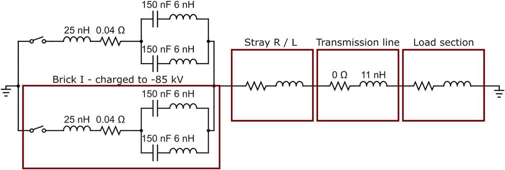
Fig. 2. Equivalent circuit diagram of the X-pinch and its respective components. The inductance of the MITL was modeled as arising from two coaxial cylinders discharging in parallel.
Fig. 3. Short-circuit current measurement with the load replaced by an M6 bolt. Nonintegrated Rogowski data were measured by a coil located within the recess of the Dry Pinch I top plate (depicted in blue). The oscillatory signal observed at the beginning of the Rogowski data is the noise caused by the switch firing. The red line corresponds to the current calculated as a cumulative integral of the nonintegrated Rogowski data.
Fig. 4. The x-ray sensitivity of the Fuji-IP MS image plate (plotted in black) and the sensitivity of the Kodak DEF (plotted in red). Data are taken from experiments and modeling by Meadowcroft et al. 19 and Henke et al. 20
Fig. 5. Transmission profile of metal filters applied to (a) a stainless steel pinhole array target and (b) diamond photoconductive detectors and silicon x-ray diodes.
Fig. 6. Temporally gated optical emission emanating from the load captured every 20 ns with 5 ns exposure time. The initial frames show wire expansion followed by magnetic compression and a micropinch formed at t = 120 ns. The timing of the frame showing the micropinch formation coincided with the emission recorded by the x-ray diodes to within the interframe time. The contrast is optimized for each image separately to highlight the morphology of the X-pinch.
Fig. 7. Timing of all data in plots (a)–(d) is offset such that the current waveforms of all measurements coincide at 5 kA. (a) Current derivative time series measured by a nonintegrating Rogowski coil and smoothed by a 100-point (20 ns) moving-average filter. (b) Numerically integrated current waveforms of 17 back-to-back shots using the X-pinch driver with 4 × 30 µ m2 silver wire load and 85 kV charging voltage. On average, a peak current of 127 kA is achieved, with a 10%–90% rise rate of 0.45 kA/ns. The red arrow denotes the visual location of the “inductive dips.” (c) The lines in the plot correspond to a signal measured by a beryllium-filtered PCD located 650 mm from the X-pinch in four separate shots (each shown in a different color). Dashed lines denote the simultaneous Rogowski coil measurement of dI /dt . In each of the four Rogowski waveforms, there is a second oscillatory structure—an “inductive dip” corresponding to a sudden change in the inductance during the pinching process. (d) Close-up of the PCD signals in (c). On average, the standard deviation between the timing of a maximum in the PCD signal and the onset of an inductive dip in the current waveform was 4.6 ns. (e) Example of a current waveform plotted alongside signals obtained by diamond PCDs and silicon AXUVs showing the simultaneity of the inductive dip and the x-ray emission. The FWHM of the highest x-ray burst is τ FWHM = 1.1 ns as measured by all PCDs and AXUV SiDs.
Fig. 8. Images of a 4 × 30 µ m2 aluminum X-pinch recorded on a Fuji-BAS MS image plate. All line plots are corrected for the magnification of the respective point-projection schemes. (a) Mesh made of 100 µ m thick stainless steel with holes 200 µ m in diameter positioned 200 mm from the X-pinch and 250 mm from the image plate. The entire mesh is covered with a 12.5 µ m Ti filter with three additional filters glued to the mesh: 6.5 µ m Al covering the right half of the mesh, and two strips of 25 µ m Ag and 7 µ m Cu covering the top and bottom. (b) Image of a USAF resolution chart positioned 210 mm from the X-pinch and 920 mm from the image plate covered by a 12.5 µ m Ti filter. (c) An aluminum flyer stripline positioned at 1130 mm from the X-pinch and 1000 mm from the image plate. (d) Line plot along the white line delineated in (a), in which the arrowhead indicates the direction of the line plot. (e) Line plot along the white line delineated across the USAF resolution chart in (b). The characteristic size of the hard x-ray source is estimated from the intensity fall-off on a sharp feature. (f) Photograph of the aluminum flyer in the same orientation as used for the point-projection radiograph shown in (c).
Fig. 9. (a) An x-ray radiograph of a USAF target covered by a 12.5 µ m Ti filter positioned 210 mm from the X-pinch and 920 mm from the film plate. The image was recorded on a Kodak DEF film plate to selectively image soft x-ray radiation (see Fig. 4 ). (b) and (c) Vertical and horizontal lineouts of a selected element averaged over 20 neighboring bins to improve the signal-to-noise ratio. The rising and falling edges of the elements imply a soft x-ray source size of ∼10 µ m. The oscillatory features around the edges are caused by the graininess of the film.
Fig. 10. Radiograph of an aluminum step-wedge spanning thicknesses from 100 to 1500 µ m in increments of 100 µ m. Signal spatially integrated over the area of respective steps is depicted by a red scatter plot. Error bars on the measured data points are calculated as the difference between the maximum and minimum pixel values in the averaging area. Optimization of a bremsstrahlung-like spectrum to match the transmitted signal yields an approximate temperature of 5870 eV. Dashed lines proportional to the transmission coefficients for energies corresponding to the K-shell emission lines of silver are included to highlight that the line emission is not the dominant process at low thicknesses, but can explain the signal at high step thicknesses.
Fig. 11. Measurement of the X-pinch emission for silver and tungsten wire loads by a convex LiF spectrometer recorded on image plates. The LiF crystal was covered by a 12.5 µ m titanium filter. The silver spectrum was obtained at a central Bragg angle of θ = 15° and the tungsten spectrum at an angle of θ = 20°. The red line in the silver spectrum denotes the signal–noise boundary: signal is only recorded to the right of the boundary. The red markers at the bottom of the spectra denote 1 keV intervals and highlight the spatial nonlinearity of the recorded spectra.


Set citation alerts for the article
Please enter your email address

© Copyright 2018-2021 | Chinese Laser Press. All Rights Reserved 沪ICP备15018463号-20