Kai-Wei Zhao, Jui-Wen Pan. Efficiency balance of a light guide plate with microstructures for a see-through head-mounted display[J]. Chinese Optics Letters, 2016, 14(2): 022201
Copy Citation Text
The efficiency balance phenomenon for see-through head-mounted displays with different microstructure conditions can be found both theoretically and using optical simulation software. A simple mathematical calculation is used to determine the relationship between the real image (see-through function) energy and the virtual image energy. The simulation is based on factors taken from previous research studies. It is found that the balance value of the optical efficiency remains almost constant (66.63% to 67.38%) under different microstructure conditions. In addition, suitable conditions for the microstructures in see-through head-mounted displays for daily applications can be predicted.
Head-mounted displays (HMDs) have been studied for several years[1], but with the maturing of technology of the internet of things (IOT) they have recently become more popular. HMDs are now used in many fields such as in commercial entertainment, military defense, and medical applications[2]. The see-through function is important in some applications. In the see-through HMDs a virtual image is superimposed on the real world scene, which can allow the users to observe digital information and real word information at the same time[3]. There are several designs for see-through HMDs[4] with the see-through function based on the design of the image output region. A semireflective coating is usually used in such designs. For example, Amitai et al.[5,6] designed a see-through HMD based on a light guide substrate with an array of partially reflecting surfaces. The disadvantage of this semireflective coating is the large loss of energy due to the low transmittance, which is why designs using total internal reflection (TIR) are presented. For example, Hung et al.[7] designed a see-through HMD based on a light guide plate with microstructures that took advantage of TIR to extract the virtual image rays. Although this design could decrease the loss of virtual image energy[8], the loss of the real world image energy was not considered. There are two important features to be considered in see-through HMDs, the visibility of the virtual image, and the visibility of the real image. Both of these items should be considered when a see-through HMD is designed. The relationship between the real image energy and the virtual image energy is very important in HMD applications.
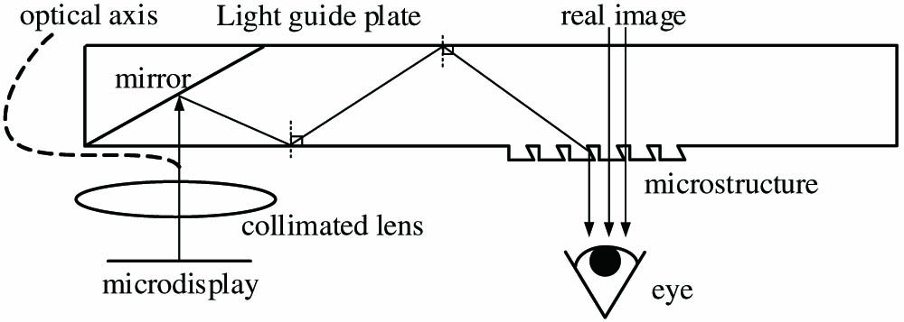
In this study, a simple mathematical calculation is used to determine the relationship between the real image (see-through function) energy and the virtual image energy for different microstructure conditions. Moreover, the efficiency balance phenomenon for different microstructure conditions can also be found theoretically and with optical simulation software. This balance phenomenon can be proved in different ways. Moreover, suitable conditions for microstructures for a see-through HMD for daily applications can be predicted. In order to facilitate the analysis, we take as an example from previous research an optical see-through HMD that utilizes a light guide plate with microstructures[7]. As shown in Fig. 1, the rays from the microdisplay propagate into the light guide plate after passing through the eyepiece, where they are reflected by a mirror and then guided by TIR by striking the microstructures and then finally directed to the viewer’s eye. The ambient rays propagate into the light guide plate and then to be extracted to the viewer’s eye through the gaps between the microstructures and the flat regions of the microstructures connected to the light guide plate.
Figure 1.Layout of the see-through HMD taken from previous studies.
Thus, the flux of the rays extracted from the light guide plate is related to the distribution density of the microstructures. The optical efficiency is defined as a percentage of the flux of the rays extracted from the light guide plate divided by the flux of the rays entering the light guide plate. The optical efficiency is related to the distribution density of the microstructures. This relationship between them is discussed below.
Sign up for Chinese Optics Letters TOC. Get the latest issue of Chinese Optics Letters delivered right to you!Sign up now
The feature of interest here is the size and distribution conditions of the microstructures used in the see-through HMD. For the virtual image, the rays from the microdisplay are directed to the viewer’s eye from the microstructures by TIR. For the see-through function, the real image is produced by the passage of the ambient rays through the gaps between the microstructures and the flat regions of the microstructures connected to the light guide plate to the viewer. According to the definition of the optical efficiency, the tendency of the optical efficiency can be expected by the distribution density of the microstructures. Regardless of the shape of the microstructures, when the density increases, the optical efficiency of the virtual image increases, while in contrast the optical efficiency of the real image decreases.
In order to facilitate the discussion, a magnified image of the trapezoidal microstructures designed in a previous study[7] is shown as an example in Fig. 2.
Figure 2.Layout of trapezoidal microstructures shown in previous research: (a) the total distribution area of the microstructures and (b) a magnified image.
Figure 2(a) shows the total distribution area of the microstructures labelled . As can be seen in Fig. 2(b), the rays from the microdisplay are reflected by TIR to strike the surface defined as . The area of the gaps between the microstructures is defined as . The flat region of the microstructures connected to the light guide plate is defined as . The ambient rays strike areas and . The probability of rays striking surface is . Because the probability should consider the shielding effect of side , the probability is defined as divided by . As shown in Fig. 3, the surface is the projection of surface on side . The angle is the guiding angle for the rays guiding in the light guide plate by TIR. The relation between surface and is shown in Eq. (1). The probability of rays striking areas and is , which is defined as divided by . The relationship between the optical efficiency and the probability is positive[9], as follows:
In order to calculate the area, the lateral (x direction) size of the microstructure is defined as , and the gap between the microstructures is defined as . The length of the distribution area of the microstructures is defined as and the width is defined as . The longitudinal (y direction) size of the microstructure is equal to . The distribution density of the microstructures can be written as follows: The lengths of surfaces , , and are also equal to . The width of surface is defined as side and the width of area is defined as side . The two angles of the microstructures are and , respectively. Side and side can be derived according to the following trigonometric functions[10]:
According to the above, surfaces , , , and are Thus, under the efficiency balance condition, we find that the optical efficiency of the virtual image is equal to the optical efficiency of the real image when is equal to Substituting Eqs. (1)–(9), and (10) into Eq. (11), Eq. (12)can be derived as follows: In Eq. (12), the relationship between and is derived to find the relationship between the lateral size of the microstructures and the gap between them, when the lengths of , , and are all equal to . Moreover, when is equal to , the relationship between the lateral size and the gap between the microstructures is expressed as a ratio. The ratio coefficient is related to the two angles and of the microstructure and the guiding angle . The guiding angle is decided. When the shape of the microstructure is decided, the two angles and are also decided. Thus, the ratio coefficient is a constant, The probabilities P1 and P2 are derive as follows: According to Eq. (13), the values of and are not related to and when is equal to . In other words, the balance between the optical efficiency of the virtual image and the optical efficiency of the real image is independent of the lateral size and the gap between the microstructures. The values of and are only related to and when is equal to . Because the shape of the microstructure is decided, the angle is also decided. Thus, the values of and are constant when is equal to . The balance between the optical efficiency of the virtual image and the real image is also constant, as demonstrated in Eq. (4).
The Light Tools[11] simulation software is used to obtain the simulated optical efficiency values for the virtual image and the real image under different microstructure conditions, and analyze the balance between them. In the simulation software, the parameter for the distance between the two microstructures is the space as shown in Fig. 2(b). The relationship between the lateral size , gap , and space is expressed as According to Eq. (14), when the lateral size is decided, the gap can be controlled by the space . We change the distribution density of the microstructures by changing the lateral size and the space . The shape of the microstructure is already decided, so the two angles and are also decided. The values of angles and are 40.89° and 60°, respectively. Figure 4 shows the simulation results under different microstructure conditions. Lateral sizes of 100, 90, 80, 70, 60, and 50 μm corresponding to the different space are simulated for analysis.
Figure 4.Simulated values of the optical efficiencies of the virtual image and the real image under different microstructure conditions.
Under the same microstructure condition, the relationship between the optical efficiency and can be found as shown in Fig. 4. For example, when the lateral size is 50 μm, and is varied from 50 to 100 μm, the optical efficiency of the virtual image varies from 67.50% to 34.89%, and the optical efficiency of the real image varies from 67.26% to 80.51%. The variation of is 50 μm and the variation of the optical efficiencies of the virtual image and the real image are 32.61% and 13.25%, respectively. When is varied from 200 to 250 μm, the optical efficiency of the virtual image varies from 18.93% to 15.28%, and the optical efficiency of the real image varies from 91.84% to 93.44%. The variation of is also 50 μm and the variation of the optical efficiency of the virtual image and the real image are 3.65% and 1.6%, respectively. Obviously, when the variation of is the same, the variation of the optical efficiency is larger when gets smaller. In other words, under the same microstructure conditions, the optical efficiency is more sensitive to the variation of when it gets smaller. Moreover, under different microstructure conditions, the relationship between the optical efficiency and the space can also be found, as shown in Fig. 4. For example, when the lateral size is 50 μm, and is varied from 50 to 250 μm, the optical efficiency of the virtual image varies from 67.50% to 15.28% and the optical efficiency of the real image varies from 67.26% to 93.44%. The variation of is 200 μm, and the variation of the optical efficiencies of the virtual image and the real image are 52.22% and 26.18%, respectively. When the lateral size is 100 μm and is varied from 100 to 300 μm, the optical efficiency of the virtual image varies from 67.20% to 26.04% and the optical efficiency of the real image varies from 66.91% to 88.72%. The variation of is also 200 μm, and the variation of the optical efficiencies of the virtual image and the real image are 41.16% and 21.81%, respectively. Comparison of the two microstructure conditions under the same variation of shows that the variation of the optical efficiency is larger when the lateral size is smaller. In conclusion, under the different microstructure conditions the optical efficiency is more sensitive to the variation of when the lateral size is smaller.
In short, the optical efficiency of the virtual image decreases with increasing , but the optical efficiency of the real image increases. These results are consistent with our expectations. The balance value between the optical efficiency of the virtual image and the optical efficiency of the real image is constant under different microstructure conditions. As our expectation, the balance value is independent of the lateral size of the microstructure and the gap between the microstructures.
The results related to the balanced efficiency are summarized from Fig. 4 and shown in Table 1. According to Eqs. (3), (12), and (13), the balance of the optical efficiency and the ratio coefficient of lateral size and gap both remain constant when the shape of the microstructure is decided. As can be seen in Table 1, the balance in the optical efficiency and the ratio coefficient of lateral size and gap remain almost constant under different microstructure conditions. The balance value of the optical efficiency remains around 66.63% to 67.38%, and the ratio coefficient of lateral size and gap is kept around to . However, there is a little acceptable error obtained with the Monte Carlo ray tracing method[12]. Thus, the balance value of the optical efficiency and the ratio coefficient can be regarded as constants. The simulation results are consistent with the theoretical results. The efficiency balance can be found for different microstructure conditions, both theoretically and with optical simulation software. Moreover, the maximum value of the optical efficiency of the virtual image is equal to the minimum value of the optical efficiency of the real image. In previous studies, because side and side are equal[7], gap is zero when the optical efficiency of the virtual image is largest and the optical efficiency of the real image is at its minimum. Thus, the real image rays come only from the flat region of the microstructures connected to the light guide plate under the condition of balanced efficiency.
Lateral size a (μm)
Space d (μm)
Gap b (μm)
Ratio of a and b (b/a)
Balance value of the optical efficiency (%)
100
100.10
0.11
1.10×10³
67.38
90
90.00
0.10
1.11×10³
66.95
80
80.90
0.09
1.12×10³
67.28
70
70.70
0.07
1.00×10³
66.63
60
60.70
0.07
1.16×10³
67.00
50
50.60
0.06
1.20×10³
67.06
Table 1. Summary of the Efficiency Balance for Different Microstructure Conditions
In fact, when the user uses the see-through HMD capability, the intensity of the ambient rays is always stronger than the intensity of the rays from the microdisplay. The visibility of the virtual image is not good when the optical efficiency of the virtual image is equal to the optical efficiency of the real image. The larger value of visibility means there is a better HMD visibility. The visibility is defined as the efficiency of virtual image divided by the efficiency of real image , Thus, for daily applications, it is necessary to have a higher optical efficiency of the virtual image and a lower optical efficiency of the real image, as indicated by the red dashed line in Fig. 5. Because the optical efficiency is more sensitive to the variation of when the lateral size is smaller, we take the larger lateral size of 100 μm for the example that appears in Fig. 5. The red dashed line is the fitting curve for the simulation data. The slanted line area shows the conditions suitable for a see-through HMD used for daily applications. In the previous study, the shape of the microstructure is difficult for mold-lifting. However, the shape of the microstructure can be manufactured by some method. According to the method Lee et al.[13] demonstrated, the minimum gap between two microstructures is 10 μm. Thus, the feasible region in Fig. 5 shows the feasible condition of the previous design. In this feasible condition, the optical efficiency of the virtual image is lower than the optical efficiency of the real image. The visibility is not good. Due to the feasible condition, the suitable conditions for a see-through HMD used for daily applications cannot be found in the previous design.
Figure 5.Suitable conditions for a see-through HMD for daily applications, feasible condition, and visibility for the previous design; lateral size of 100 μm.
In conclusion, in many designs for see-through HMDs, semireflective coatings are used to achieve a balanced efficiency, but in this study we examine the efficiency balance phenomenon obtained with different microstructure conditions, theoretically and with optical simulation software. The different intensities between the ambient rays and the rays from the microdisplay are considered when defining suitable conditions for daily applications. Suitable conditions were not found in a previous study[7]. A better design for see-through HMDs should be developed in the future.
Kai-Wei Zhao, Jui-Wen Pan. Efficiency balance of a light guide plate with microstructures for a see-through head-mounted display[J]. Chinese Optics Letters, 2016, 14(2): 022201