• Chinese Journal of Lasers
  • Vol. 48, Issue 13, 1301003 (2021)
Jun Qi, Yonggang Zou*, Jie Fan**, Jingjing Yang, Ying Liu, and Xiaohui Ma
Author Affiliations
  • State Key Laboratory of High Power Semiconductor Laser of Changchun University of Science and Technology, Changchun, Jilin 130022, China
  • show less
    DOI: 10.3788/CJL202148.1301003 Cite this Article Set citation alerts
    Jun Qi, Yonggang Zou, Jie Fan, Jingjing Yang, Ying Liu, Xiaohui Ma. 1064 nm Wide-Ridge Waveguide Semiconductor Laser with Lateral Microstructure[J]. Chinese Journal of Lasers, 2021, 48(13): 1301003 Copy Citation Text show less
    Lateral microstructure wide-ridge waveguide semiconductor laser. (a) Device structure diagram; (b) SEM image of lateral microstructure wide-ridge waveguide; (c) packaged device diagram
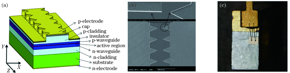
    Fig. 1. Lateral microstructure wide-ridge waveguide semiconductor laser. (a) Device structure diagram; (b) SEM image of lateral microstructure wide-ridge waveguide; (c) packaged device diagram
    Modes distribution diagram of WR-LD
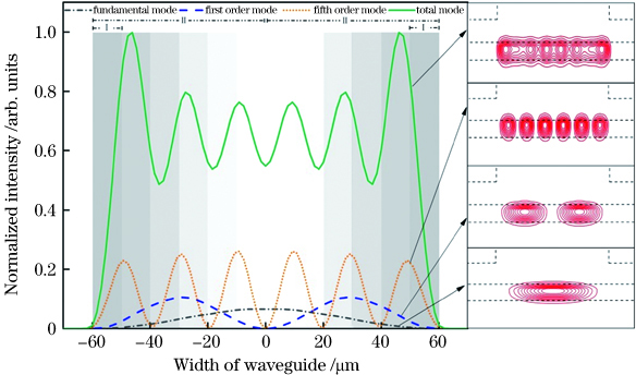
    Fig. 2. Modes distribution diagram of WR-LD
    Relationship between the lateral microstructures of different widths and the optical field distribution of each lateral mode. (a)--(c) Lateral microstructure width is 0 μm; (d)--(f) lateral microstructure width is 20 μm; (g)--(i) lateral microstructure width is 50 μm
    Fig. 3. Relationship between the lateral microstructures of different widths and the optical field distribution of each lateral mode. (a)--(c) Lateral microstructure width is 0 μm; (d)--(f) lateral microstructure width is 20 μm; (g)--(i) lateral microstructure width is 50 μm
    Mode loss graphs. (a) Relationship between the lateral microstructures of different widths and the loss of each lateral mode; (b) relationship between the lateral microstructure of different widths and the mode loss difference
    Fig. 4. Mode loss graphs. (a) Relationship between the lateral microstructures of different widths and the loss of each lateral mode; (b) relationship between the lateral microstructure of different widths and the mode loss difference
    Near-field spot patterns. (a) WR-LD three-dimensional near-field spot pattern; (b) LMWR-LD three-dimensional near-field spot pattern; (c) two-dimensional near-field distribution pattern
    Fig. 5. Near-field spot patterns. (a) WR-LD three-dimensional near-field spot pattern; (b) LMWR-LD three-dimensional near-field spot pattern; (c) two-dimensional near-field distribution pattern
    Schematic diagram of lateral divergence angle
    Fig. 6. Schematic diagram of lateral divergence angle
    Device characteristic curves. (a) L-I-V characteristic curves; (b) electro-optic conversion efficiency characteristic curves
    Fig. 7. Device characteristic curves. (a) L-I-V characteristic curves; (b) electro-optic conversion efficiency characteristic curves
    NumberTypeMaterialThickness d /μmDoping level /cm-3Average refractive index
    1CapGaAs0.20002×10203.48
    2p-claddingAl0.5Ga0.5As1.00001×10183.23
    3p-waveguideAl0.3Ga0.7As0.15003.34
    4Active regionGaAs0.00173.66
    5Ga0.17As0.83P0.0060
    6In0.34Ga0.66As0.0060
    7Ga0.17As0.83P0.0060
    8GaAs0.0017
    9n-waveguideAl0.3Ga0.7As0.45003.34
    10n-claddingAl0.5Ga0.5As1.00001×10183.23
    Table 1. Structure parameters of epitaxial layer
    Jun Qi, Yonggang Zou, Jie Fan, Jingjing Yang, Ying Liu, Xiaohui Ma. 1064 nm Wide-Ridge Waveguide Semiconductor Laser with Lateral Microstructure[J]. Chinese Journal of Lasers, 2021, 48(13): 1301003
    Download Citation