
Yu-Xiang Zhang, Yi-Tian Peng, Hao-Jie Lang. Controllable nano-friction of graphene surface by fabricating nanoscale patterning based on atomic force microscopy [J]. Acta Physica Sinica, 2020, 69(10): 106801-1
- Acta Physica Sinica
- Vol. 69, Issue 10, 106801-1 (2020)
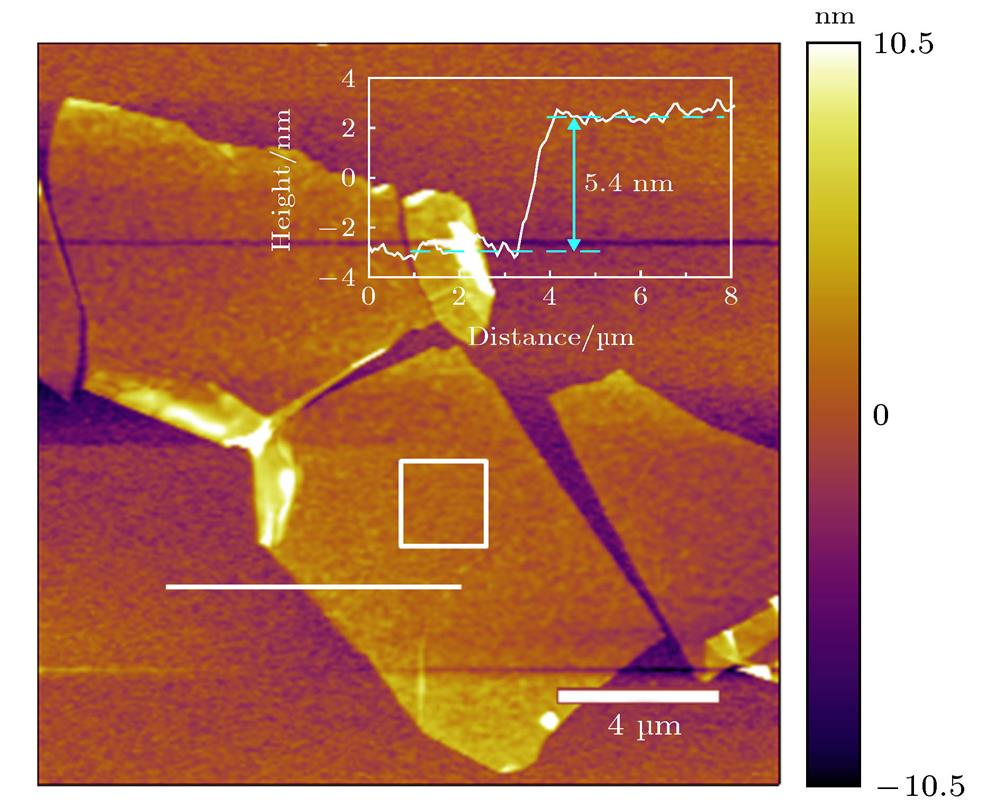
Fig. 1. AFM topographic image with height of graphene obtained by mechanical stripping.
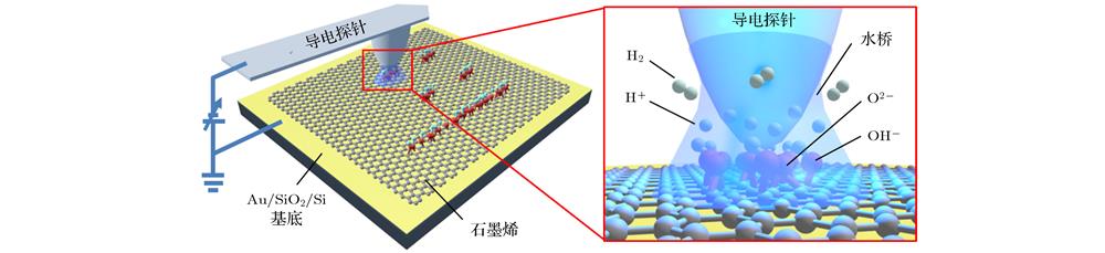
Fig. 2. Schematic diagram of AFM setup for processing nanometer pattern ongraphenesurface.
Fig. 3. Nano-friction of graphene surface was regulated by oxidation points at a constant voltage and different contact time: (a) Friction image; (b) topography image; (c) CPD image; (d)−(f) corresponds to the changes in friction, height and CPD along each row in (a)−(c), respectively.
Fig. 4. Nano-friction of graphene surface was regulated by oxidation points at a constant contact time and different voltages: (a) Friction image; (b) CPD image; (c) and (d) correspond to the changes in friction and CPD along each row in (a) and (b), respectively.
Fig. 5. Nano-friction of graphene surface was regulated by oxidation line at a constant load and different voltages: (a) Friction image; (b) topography image; (c) CPD image; (d)−(f) corresponds to the changes in friction, height and CPD along red line in (a)−(c), respectively.
Fig. 6. Nano-friction of graphene surface was regulated by oxidation line at a constant voltage and different loads: (a) Friction image; (b) topography images; (c) and (d) correspond to the change in friction and height of the oxidation line when the load is 10 nN and 100 nN, respectively.
Fig. 7. Nano-friction of thick graphene surface was regulated by oxidation line: (a) AFM topography image of thick graphene. The inset shows the height profile along white line. (b) and (c) are the friction and topography image of the white box in (a) after etching , respectively; (d) and (e) correspond to the change in friction and height of the oxidation line.
Fig. 8. Lithography of graphene nanoscale patterns: (a) Friction image; (b) topography images; (c) CPD image.

Set citation alerts for the article
Please enter your email address
© Copyright 2018-2021 | Chinese Laser Press. All Rights Reserved 沪ICP备15018463号-20