Abstract
In this Letter, we propose a broadband near-infrared (NIR) absorber based on the phase transition material VO2. By designing different arrangements of the VO2 square lattice at high and low temperatures on fused silica substrates, the absorption rate reaches more than 90% in the entire 1.4–2.4 μm range. Using a finite-difference time-domain simulation method and thermal field analysis, the results prove that the absorber is polarization-independent and has wide-angle absorption for incident angles of 0°–70°. The proposed absorber has a smoother absorption curve and is superior in performance, and it has many application prospects in remote sensing geology.The research on broadband absorbers has made great progress in recent years, especially the metamaterial absorbers. Metamaterials[1,2] are special synthetic materials; the physical properties of the metamaterial not only depend on the intrinsic properties of the composite materials, but also on its micro-nano structure. Most of its superior performance and physical properties cannot be obtained by existing materials.
In previous studies, the special physical properties such as negative refractive index[3–5], super-absorption[6–9], asymmetric transmission[10,11], and negative Poisson’s ratio[12,13] have been realized. The realization of these characteristics shows a close relationship between the micro/nanostructures and the arrangement of cells. By choosing different materials and designing different structures and feature sizes, an absorber can be obtained with different working bands and properties.
In the studies on metamaterial absorbers, most researchers have realized perfect absorption at a certain wavelength or some wavelength bands by designing micro/nanostructures on the surface of the metal–dielectric–metal composite structure. Lei et al.[14] designed a thermally tunable broadband absorber based on the structure by combining resonators with different-sized cubes in the unit cell, and it achieved over 90% absorption in the near-infrared (NIR) to mid-infrared region. This structure has superior characteristics but needs precise fabrication and measurement. Other researchers have proposed metal and dielectric multilayer composite thin film planarized absorbers that realize broadband absorption by the alternate stacking of metallic and dielectric planes. To achieve broadband perfect absorption, Zhong et al.[15] reported a planarized absorber based on a 32-layer ultra-thin film structure. Such an absorber requires repeated coating, and the film thicknesses need precise control, which is difficult to achieve. Some researchers have achieved broadband perfect absorption at a certain wavelength band by designing a pyramid-like structure. Chen et al.[16] reported a nanowire-based absorber made of gold nanowires embedded in a truncated pyramid silica host and achieved near-perfect absorption in an ultra-broadband from 200 nm to 600 nm. The pyramid structure has especially high requirements of the lithography process in the actual preparation. The atmospheric window of 1.4–2.4 μm is called the NIR window, which is mainly used in electromagnetic energy detection, geological survey, resource exploration, etc. At present, there is little research on the absorber in this band. Therefore, it is particularly important to design a high-performance metamaterial absorber in the 1.4–2.4 μm band.
Sign up for Chinese Optics Letters TOC. Get the latest issue of Chinese Optics Letters delivered right to you!Sign up now
To solve the problems of low absorption, non-adjustable absorption, and polarization sensitivity of absorbers, we propose an NIR absorber in this Letter based on the phase transition of vanadium dioxide () at 68°C. The resistivity, magnetic susceptibility, infrared transmission, and other physical properties[17] of are changed suddenly during the phase transition at a sub-picosecond timescale[18]. Broadband absorption is achieved by designing different arrays of the square lattices at high and low temperatures. Further, using the finite-difference time-domain (FDTD) method and thermal analysis, the cross array absorber can realize the broadband polarization-independent properties. In the 1.4–2.2 μm band, the absorption rate is stabilized at around 85%, which can be applied in fields where the absorption rate is strict.
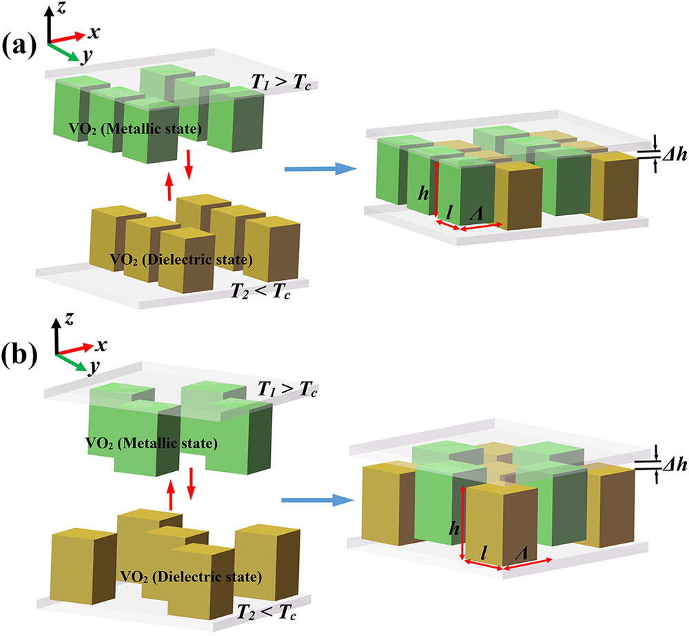
has many excitation modes, such as thermally induced phase transition, electrically induced phase transition, and photo-induced phase transition. This study uses the characteristics of its thermally induced phase transition, i.e., the metallic state in the tetragonal rutile phase and the dielectric state in the monoclinic phase can be changed reversibly as a function of temperature. With the change in the crystal structure of , its photoelectric characteristics also change. The strong absorption of light by the dielectric state changes to the inhibition of light absorption by the metallic state so that the dynamic regulation of the absorption rate of the absorber can be realized. The broadband perfect absorption of the absorber is realized by the excitation of magnetic resonance in metallic state and dielectric loss in dielectric state [19]. In order to control the temperature precisely, two square lattices with the same height, length, and period are arranged on two fused silica glasses, which can be fabricated by thin film deposition, photolithography, and etching techniques. Then, the interferometric alignment technique can be used to insert and combine the upper and lower layers to form a new structure operating at both high and low temperatures, as shown in Fig. 1. The linear array and cross array of the square lattices are, respectively, shown in Figs. 1(a) and 1(b). The square lattices are chosen for a smoother absorption curve, while the symmetry of these two structures is designed to facilitate the absorption of different polarized light. The larger glass substrates are fabricated, making it easier to control the temperature of the different substrates with a temperature controller. The temperatures of the two glasses with the square lattices are maintained near the phase transition temperature ( and ). The length of the square lattice is represented by , and its height and period are denoted by and , respectively. Moreover, represents the distance between two linear or cross arrays in the different substrates.

Figure 1.(a) Schematic of the linear array absorber. (b) Schematic of the cross array absorber.
According to the energy conservation rule[20], , where , , and are the spectral absorption, reflection, and transmission, respectively. In order to minimize the reflection, impedance matching between the metamaterial and free space is necessary. The metamaterial impedance is given by , where is the impedance of free space, and is the relative impedance of metamaterial. When the light is incident normally, the reflection and transmission are, respectively, described by the following equations[21]:
Here, is the frequency of the incident light. In the equation for , is the imaginary part of the refractive index, is the thickness of the metamaterial, and is the speed of light in vacuum. Therefore, the relative permeability and relative permittivity will vary with the geometric parameters of the structure, and when , the reflection is almost zero to achieve perfect absorption.
If the light is non-normal incidence, the reflection is different from the normal incidence. So, the reflection for TE polarization and TM polarization can be expressed as[22]where is the incident angle of the light, and is the refractive index of . Therefore, with the change of light incident angle, the reflection will also change, thus having a certain effect on the absorption rate.
From the equations, we observe that the impedance of the absorber is mainly influenced[23] by the length, height, period, and the different working temperatures of the square lattices. Lumerical FDTD Solutions is used to simulate the absorption of light for the absorber. All simulations use auto non-uniform mesh settings. Two structures are simulated using periodic boundary conditions and Bloch boundary conditions along the and directions in the cases of normal incidence and oblique incidence, respectively, and perfectly matched layer boundary conditions along the direction by the FDTD method. Plane waves are incident to the structures along the negative direction of the axis, and the reflection and transmission are computed with a power monitor[24]. The origin of the axis is at the center of the cycle unit. When simulating using the FDTD method, the glass data is obtained from the Palik database[25], and the refractive index data of is obtained from Refs. [26,27].
To reduce the mutual influence between high temperature and low temperature in the cross array absorber, it is important to prevent the square lattice from touching the upper and lower glass substrates at the same time. Considering the above situation, the distance between two lattice arrays on the substrates is 0.01 μm. The upper glass substrate thickness is set to 200 μm. By analyzing, the optimal parameters , , , , and of the linear array absorber and cross array absorber are, respectively, 1.0 μm, 1.6 μm, 1.4 μm, 80°C, 60°C and 1.0 μm, 1.4 μm, 1.4 μm, 80°C, 60°C. Please refer to Supplementary Materials[28] for detailed analysis of simulations. From Fig. 2, we observe that, compared to the linear array absorber, the absorption rate of the cross array absorber reaches 90%, and the characteristics of broadband absorption are achieved.
Figure 2.Absorption spectra of designed structures.
To ensure that the square lattices function in different states, it is necessary to analyze the thermal properties of the cross array absorber. Heat transfer between high-temperature and low-temperature occurs through thermal radiation, thermal conduction, and thermal convection in the cross array absorber. It is convenient to analyze the temperature field distribution of the absorber by selecting a cycle unit. In the ANSYS thermal analysis module, the room temperature is 20°C, the air convection coefficient is maintained at , and the material emissivity is equal to its absorptivity according to Kirchhoff’s law of thermal radiation[29]. In this study, the emissivity of dielectric state , metallic state , and glass are, respectively, 0.9, 0.5, and 0.9. The specific parameters of and glass are obtained from Refs. [30–32]. From the simulation, we observe that the temperature field distribution for the values of 0.05 μm, 0.08 μm, 0.1 μm, 0.2 μm, and 0.3 μm are similar. The temperature field distribution for is shown in Fig. 3(a). At the micro-nano scale, the heat transfer is dominated by thermal conduction, and the influence of natural convection can be neglected[33–36].
Figure 3.(a) Temperature field distribution in the cross array absorber for . (b) Absorption spectra of the cross array absorber for different .
The absorption spectra of the cross array absorber for varying from 0.01 μm to 0.3 μm, obtained by the FDTD method, are shown in Fig. 3(b). Considering the absorption spectra and manufacturing difficulty of the cross array absorber, is selected as the case where the absorption rates do not vary significantly and can achieve nearly 90% absorption rate at 1.4–2.4 μm band.
Considering the influence of mismatch between the two substrates with square lattices in the manufacturing process, the mismatch of the cross array absorber has been simulated, as shown in Fig. 4. It can be concluded that the absorption rate does not change greatly, indicating that the mismatch of the two substrates has little influence on the performance. and represent the distance of the upper layer offset along the axis and axis, respectively.
Figure 4.Absorption spectra of the cross array absorber for different offset distances.
In order to explore the sensitivity of the cross array absorber to polarization, the effect of polarization angle on the absorption property is studied, as shown in Fig. 5. At a normal incidence, the absorption is maintained at more than 80% at any polarization angle in the wavelength range of 1.4–2.4 μm. In this study, TM polarization and TE polarization correspond to the polarization angles of 0° and 90°, respectively, i.e., the electric field is parallel to the incident plane[27]. When the polarization angle changes, the absorption frequency and absorption rate of the absorber remain unchanged. This is mainly because the incident electromagnetic wave can be decomposed into TE and TM polarization waves. Meanwhile, the square lattices are symmetrical for TE and TM due to symmetry, and so the structure has similar response to TE and TM polarizations. When the light is incident on the absorber, the molecule vibrates under the influence of the electric field of the light, which hinders the propagation of the light and slows down the speed of the light. If the light passes through a centrosymmetric structure, the TE and TM polarization waves have a similar electric field distribution[37]; therefore, the speed of light is similar when passing through the structure, and the equivalent refractive indices are basically the same. Polarization angles of light have little effect on the absorption rates at incident angles between 0° and 15°. The absorption rates are polarization-dependent when the incident angle is larger than 15°. Figure 5(b) shows the influence of the polarization angle on the absorption characteristics at the incident angle of 27°. Thus, we can infer that the absorber has the characteristic of near-polarization insensitivity[38].
Figure 5.Absorption spectra of the cross array absorber at different polarization angles: (a) at a normal incidence; (b) at an incident angle of 27°.
Subsequently, we investigate the influence of the incident angle from 0° to 70° on the absorption of the cross array absorber. Figures 6(a) and 6(b) show the simulated absorption spectra at different angles of incidence under TM and TE polarization, respectively. As the angle of incidence increases, the magnetic resonance flux of the absorber decreases; thus, the absorption rate decreases[39]. Under TM polarization, as varies from 0° to 70°, the absorption rate is more than 70%, and broadband absorption is still conspicuous because of a strong magnetic resonance produced in the absorber to maintain high absorption at large incident angles[40]. With the increase in the incident angle, the absorption rate reaches a peak and is gradually red shifted. This is because the internal electric field of the dielectric state becomes stronger, and the absorption of light is enhanced. Under TE polarization, the absorption is more than 85% in the range 1.4–1.8 μm, as varies from 0° to 70°. The absorption decreases significantly as the incident angle increases because the cross array absorber is sensitive to the incident angle in the 1.8–2.4 μm band. Because of the far-field interaction between adjacent square lattices, the line-width of adjacent resonance is extended and overlapped, and broadband absorption is realized[41]. However, the change in the incident angle reduces the surface plasmon polaritons of the metallic state , interferes with the surface plasmon oscillation of metallic state at the interface between glass and metallic state , and thus affects the broadband absorption of the absorber. Overall, under TE and TM polarizations, the absorption rate still remains above 65% in the 1.4–2.4 μm band at the incident angle of 70°, and this wide-angle absorption characteristic is suitable for application in solar cells and other fields.
Figure 6.Absorption spectra of the cross array absorber at different incident angles: (a) under TM polarization; (b) under TE polarization.
Finally, to understand the intrinsic mechanism of perfect absorption, the electric and magnetic field distributions at the wavelength of 2 μm using the frequency-domain field profile monitor are presented in Fig. 7. The perfect absorption performance of the absorber mainly depends on the impedance matching in metamaterials and free space. The energy is mainly concentrated in the interior of the dielectric state and the surface of the metallic state , which means that the strong absorption is due to electric dipole resonance in the metallic state surface and dielectric loss in the dielectric state . Nevertheless, the interior of the metallic state has less energy because of the high imaginary part of its dielectric constant, and so the field penetration is smaller, and the light absorption is suppressed[21]. The broadband absorption stems from the magnetic resonance of the plasma on the surface of metallic state and the high loss absorption of dielectric state . In the 1.4–2.4 μm band, the absorption coefficient of the dielectric state gradually increases as the wavelength decreases. When the wavelength of incident light is less than 1.77 μm, the absorption is abruptly increased due to optical transition in the fundamental bandgap[42]. Under the action of an electric field, due to the hysteresis effect of dielectric conductance and dielectric polarization, electromagnetic energy has been consumed. Because of the plasma resonance at the interface between metallic state and glass, the incident light is absorbed. So the broadband absorption occurs in the metamaterial absorber.
Figure 7.Three-dimensional (3D) FDTD simulation of the electromagnetic field distribution. (a) The electric field distribution in the plane. (b) The magnetic field distribution in the plane. (c) The electric field distribution in the plane. (d) The magnetic field distribution in the plane.
In conclusion, we demonstrated an NIR absorber with broadband absorption based on the phase transition material . The optimal parameters of the absorber were obtained using the FDTD method. Two square lattice arrangements, the linear array and cross array, were designed, and the cross array absorber had a higher absorption rate of approximately 90% for linearly polarized and unpolarized infrared light in the working wavelength band. Moreover, thermal analysis using the ANSYS module proved the stability and feasibility of the structure. The absorber was polarization-independent at normal incidence, and wide-angle absorption occurred under TE and TM polarizations. Further, the electromagnetic field distribution was used to explain the absorption mechanism. This study will contribute to the development of metamaterial absorbers, which have wide applications in optoelectronic devices.
References
[1] H. Sun, L. Wang, Y. Zhang, S. Liang, J. Han, F. Lan, X. Zhou, Z. Yang. Chin. Opt. Lett., 17, 041602(2019).
[2] X. Luo, Z. Tan, C. Wang, J. Cao. Chin. Opt. Lett., 17, 093101(2019).
[3] J. B. Pendry. Science, 306, 1353(2004).
[4] M. Labidi, F. Choubani. Opt. Mater., 82, 116(2018).
[5] T. Suzuki, M. Sekiya, T. Sato, Y. Takebayashi. Opt. Express, 26, 8314(2018).
[6] Q. Feng, M. Pu, C. Hu, X. Luo. Opt. Lett., 37, 2133(2012).
[7] M. Pu, Q. Feng, M. Wang, C. Hu, C. Huang, X. Ma, Z. Zhao, C. Wang, X. Luo. Opt. Express, 20, 2246(2012).
[8] Y. Huang, J. Luo, M. Pu, Y. Guo, Z. Zhao, X. Ma, X. Li, X. Luo. Adv. Sci., 6, 1801691(2019).
[9] Y. Liu, Z. Wu, E. H. Hill, Y. Zheng. Chin. Opt. Lett., 16, 050004(2018).
[10] D. E. Fernandes, M. G. Silveirinha. J. Appl. Phys., 122, 014303(2017).
[11] D. J. Park, J. H. Shin, K. H. Park, H. C. Ryu. Opt. Express, 26, 17397(2018).
[12] L. Ai, X. L. Gao. Science, 135, 101(2018).
[13] S. A. Lurie, A. L. Kalamkarov, Y. O. Solyaev, A. D. Ustenko, A. V. Volkov. Int. J. Solids Struct., 132–133, 188(2017).
[14] L. Lei, F. Lou, K. Tao, H. Huang, X. Cheng, P. Xu. Photon. Res., 7, 734(2019).
[15] Y. Zhong, Y. Lai, M. Tu, B. Chen, S. Fu, P. Yu, A. Lin. Opt. Express, 24, A832(2016).
[16] Q. Chen, J. Gu, P. Liu, J. Xie, J. Wang, Y. Liu, W. Zhu. Opt. Laser Technol., 105, 102(2018).
[17] M. H. Lee, M. G. Kim, H. K. Song. Thin Solid Films, 290–291, 30(1996).
[18] K. Appavoo, R. F. Haglund. Nano Lett., 11, 1025(2011).
[19] H. Wang, Y. Yang, L. Wang. J. Appl. Phys., 116, 123503(2014).
[20] H. Kocer, S. Butun, Z. Li, K. Aydin. Sci. Rep., 5, 8157(2015).
[21] C. M. Watts. Metamaterials and their applications towards novel imaging technologies. Ph.D. Thesis(2015).
[22] B. Chen. Omnidirectional infrared broadband absorber based on multiplexed metal-insulator-metal structure. Master Thesis(2013).
[23] D. R. Smith, D. C. Vier, T. Koschny, C. M. Soukoulis. Phys. Rev. E, 71, 036617(2005).
[24] H. Kocer, S. Butun, B. Banar, K. Wang, S. Tongay, J. Wu, K. Aydin. Appl. Phys. Lett., 106, 161104(2015).
[25] E. D. Palik. Handbook of Optical Constants of Solids II(1998).
[26] M. J. Dicken, K. Aydin, I. M. Pryce, L. A. Sweatlock, E. M. Boyd, S. Walavalkar, J. Ma, H. A. Atwater. Opt. Express, 17, 18330(2009).
[27] Z. Liu, M. Zhao, J. Gao, Y. Li, S. Jiang. Results Phys., 7, 4222(2017).
[28]
[29] C. M. Watts, X. Liu, W. J. Padilla. Adv. Mater., 24, OP98(2012).
[30] D. W. Oh, C. Ko, S. Ramanathan, D. G. Cahill. Appl. Phys. Lett., 96, 151906(2010).
[31] K. Xu, Y. Lu, Y. Ling, Y. Qiao. Acta Photon. Sin., 44, 0531003(2015).
[32] J. Jiao, X. Wang. High Power Laser Part. Beams, 19, 1(2007).
[33] M. Wang, Z. Li. Sci. China Ser., 48, 317(2005).
[34] M. A. Gallis, J. R. Torczynski, D. J. Rader. Sensor Actuat. A Phys., 134, 57(2006).
[35] M. Goodarzi, A. D’Orazio, A. Keshavarzi, S. Mousavi, A. Karimipour. Physica A, 509, 210(2018).
[36] H. Weng, D. C. Chen. Int. J. Heat Mass Transfer, 57, 16(2013).
[37] L. Ye, X. Chen, J. Zhou, F. Han, Q. Liu. Appl. Phys. Express, 11, 102201(2018).
[38] V. G. Achanta. Prog. Quant. Electron., 39, 1(2015).
[39] P. Yang, T. Han. Acta Phys. Sin., 67, 107801(2018).
[40] J. Yang, S. Qu, H. Ma, J. Wang, Y. Pang. Opt. Commun., 402, 518(2017).
[41] F. Gao, Z. Zhu, W. Xu, J. Zhang, C. Guo, K. Liu, X. Yuan, S. Qin. Opt. Express, 25, 9579(2017).
[42] D. Fu, K. Liu, T. Tao, K. Lo, C. Cheng, B. Liu, R. Zhang, H. A. Bechtel, J. Wu. J. Appl. Phys., 113, 043707(2013).