
Jun-Jun QI, Hong-Liang LYU, Yu-Ming ZHANG, Yi-Men ZHANG, Jin-Can ZHANG. An improved direct extraction method for InP HBT small-signal model[J]. Journal of Infrared and Millimeter Waves, 2020, 39(3): 295
- Journal of Infrared and Millimeter Waves
- Vol. 39, Issue 3, 295 (2020)
Abstract
Introduction
Owing to the characteristics of high-speed and high-frequency, InP HBT has been one of the most promising devices for future applications at microwave and millimeter-wave frequencies[
With scaling down transistors’ size, in general, the structure of C-up HBT devices can ignore the extrinsic base-collector capacitance because the extrinsic area corresponding to the parasitic capacitance can be neglected[
In recent years, many methods that extract small signal model parameters have been reported, mainly including direct extraction method [
In order to overcome these difficulties, an improved direct extraction method for InP HBT small-signal model is proposed. This method in turn extracts the parameters of small-signal equivalent circuit from the peripheral elements to the internal elements. Compact with the other direct extraction methods, the method has clear extraction process, simple calculation of parameters, and few approximations calculation.
1 Small-signal equivalent circuit model
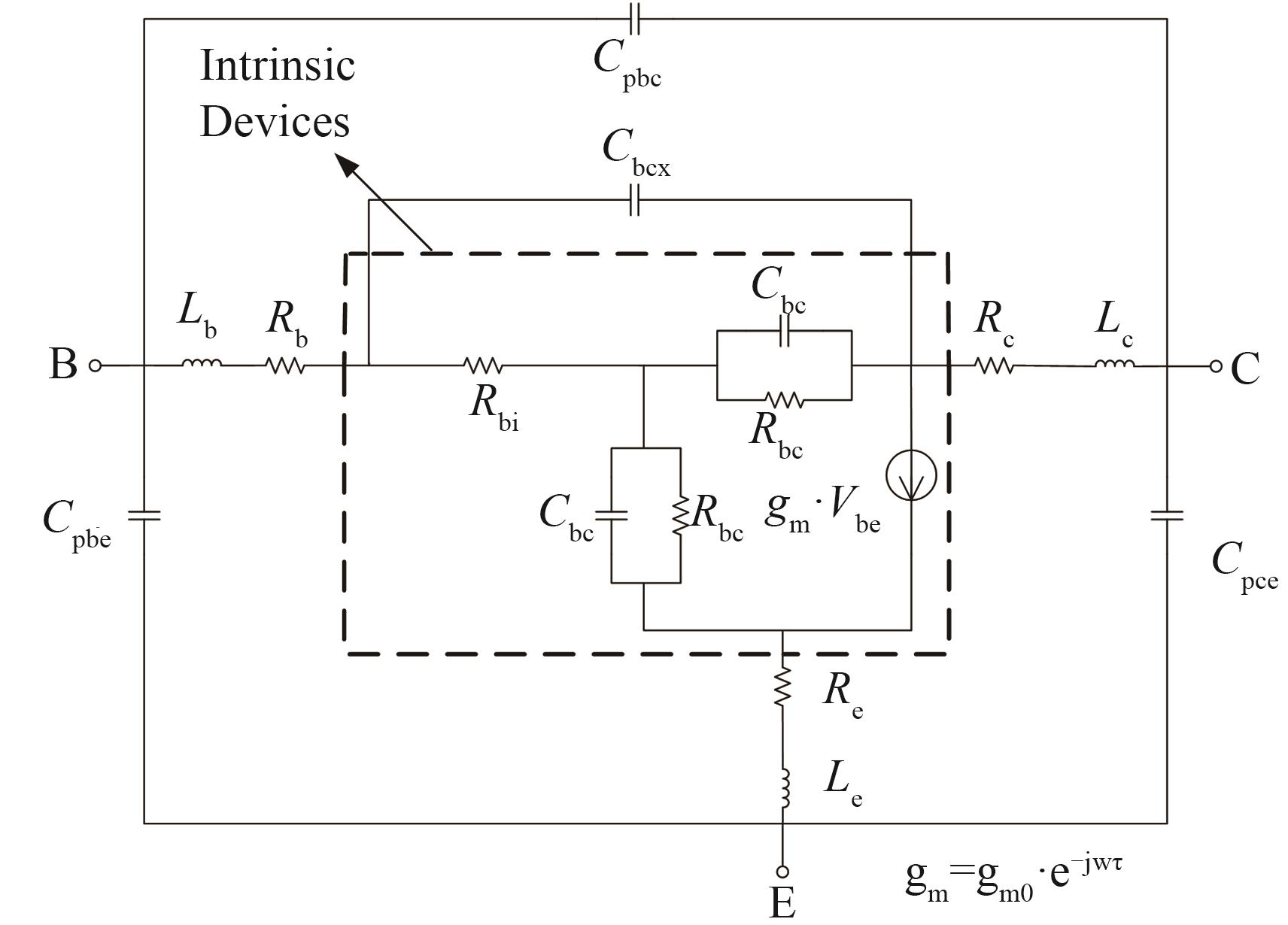
The adopted hybrid-π equivalent circuit for HBT small-signal modeling is shown in
![]()
Figure 1.HBT small-signal equivalent circuit
Intrinsic elements are supposed to be bias dependent, mainly including the dynamic base resistance Rbi, the dynamic base-emitter resistance Rbe, the base-emitter capacitance Cbe, the base-collector capacitance Cbc, the dynamic base-collector resistance Rbc, DC transconductance gm0 and delay time τ. Besides, Cbcx is extrinsic base-collector capacitance, and it is considered to be bias independent.
2 Parameter extraction procedure
2.1 Extraction of parasitic parameters and the extrinsic resistances
Pad parasitic parameters consist of parasitic capacitances and inductances which are extracted by the Open Test Structure and the Short Test Structure [
![]()
Figure 2.open-collector equivalent circuit
The Z-parameters of the open-collector equivalent circuit in
When Ib approaches ∞, Rbe and Rbc become very small at approximately 0 because the junction resistance and the junction current are inversely proportional. Moreover, with the increasing of the base current Ib, the total resistance of the base gradually approaches the base contact resistance[
The relationship between real(Z11-Z12), real(Z22-Z12) and real(Z12) and 1/Ib is linearly extrapolated to the ordinate to obtain the values of Rb, Rc and Re, as shown
![]()
Figure 3.Plots of the real part of
| parasitic parameters | Vce=2.5 V, Ic=12.5 mA |
|---|---|
| Cpbc/fF | 2.62 |
| Cpbe/fF | 15.60 |
| Cpce/fF | 16.20 |
| Lb/pH | 52.25 |
| Lc/pH | 57.75 |
| Le/pH | 8.88 |
| Re/Ω | 4.27 |
| Rb/Ω | 1.77 |
| Rc/Ω | 7.31 |
Table 1. Extraction of extrinsic parameters values
2.2 Extraction of the extrinsic base-collector capacitance
Once all the parasitic elements are de-embedded, only the extrinsic base-collector capacitance Cbcx and the intrinsic elements (inside the dashed line) are remained in the equivalent circuit, as shown in
![]()
Figure 4.equivalent circuit after de-embedding off parasitic elements
The Z-parameters of the equivalent circuit after de-embedding in
where ,,, , , and
From (10), the dynamic base resistance Rbi can be expressed as
where , and
The extrinsic base-collector capacitance can be expressed by taking the imaginary part of equation (11) equal to 0 as
![]()
Figure 5.
2.3 Extraction of the intrinsic elements
Once the parasitic elements and extrinsic base-collector capacitance is de-embedded, the remaining intrinsic elements of the small signal equivalent circuit model can be directly determined. The Z-parameter corresponding to the intrinsic circuit can be written as
From (13), the intrinsic base resistance Rbi can be expressed as
![]()
Figure 6.
![]()
Figure 7.the equivalent circuit of de-embedding
The Y parameter of the corresponding equivalent circuit (
From (15), the intrinsic elements can be expressed as
3 Results and discussion
A hybrid-π small-signal equivalent circuit with distributed base-collector capacitance effect was adopted to study the microwave and millimeter-wave behavior of the InP HBT. An improved direct extraction method has been established to accurately extract the small-signal parameters. The improved method extracts parameters from the peripheral circuit to the internal circuit and gives a clearer solution process. Extraction results of small signal equivalent circuit are depicted in
| Intrinsic parameters | Ic=2.5mA | Ic=12.5mA | Ic=22.5mA |
|---|---|---|---|
| Cbcx/fF | 49.21 | 35.60 | 58.31 |
| Rbi/Ω | 36.22 | 8.32 | 2.45 |
| Rbe/Ω | 2497.68 | 121.02 | 113.50 |
| Rbc/Ω | 1.90×10⁴ | 2.66×10⁴ | 1.04×10⁴ |
| Cbc/fF | 32.03 | 18.26 | 16.59 |
| Cbe/fF | 145.30 | 718.85 | 915.30 |
| gm0/S | 0.08 | 0.60 | 1.19 |
Table 2. Extraction of Intrinsic Parameters at Vce=2.5V
![]()
Figure 8.Measured and calculated S-parameters of 1×15 μm2 InP HBT between 100 MHz~40 GHz
However, the Smith plots of S parameters do not clearly reflect agreement of fit between measured and calculated data. The residual error between the measured results and the calculated results are quantified using the following equation [16]
where N is the number of frequency points, Sijm (fk) and Sijc (fk) are the measured and calculated S-parameters at frequency fk, respectively. The residual errors between the measured and modeled S-parameters are around 3.3~3.8%.
4 Conclusion
An improved direct extraction method for the hybrid-π small-signal equivalent circuit with the base-collector capacitance effect has been proposed. The extracting process of this method, which extracts parameters in turn from the peripheral parasitic elements to the intrinsic internal elements, is clearer than other direct extraction methods. Furthermore, this method can extract all intrinsic parameters directly by the equation without approximation and numerical optimization. Good agreement is obtained between calculated and measured results for an InP HBT with 1×15 μm2 emitter area over a wide range of bias points up to 40GHz.
References
[1] M Hossain, K Nosaeva, B Janke. A G-Band High Power Frequency Doubler in Transferred-Substrate InP HBT Technology. IEEE Microwave and Wireless Components Letters, 26, 49-51(2016).
[2] J Yun, D Yoon, H Kim. 300-GHz InP HBT oscillators based on common-base cross-coupled topology. IEEE Transactions on Microwave Theory and Techniques, 62, 3053-3064(2014).
[3] Z Ao, Z Yi-Xin, W Bo-Ran. An approach to determine small-signal model parameters for InP HBT up to 110 GHz. Journal of Infrared and Millimeter Waves(2018).
[4] Y Sun, Z Liu, X Li. Distributed Small-signal Equivalent Circuit Model and Parameter Extraction for SiGe HBT. IEEE Access, 1-1(2019).
[5] S Yamahata, K Kurishima, T Kobayashi. InP/InGaAs collector-up heterojunction bipolar transistors fabricated using Fe-ion-implantation(1995).
[6] T S Horng, J M Wu, H H Huang. An extrinsic-inductance independent approach for direct extraction of HBT intrinsic circuit parameters. IEEE Transactions on Microwave Theory and Techniques, 49, 2300-2305(2001).
[7] A Oudir, M Mahdouani, S Mansouri. Small-signal modeling of Emitter-up HBT using an improved analytical approach. Application to InGaAlAs/GaAsSb/InP DHBT with strained base. Solid-State Electronics, 54, 67-78(2010).
[8] T K Johansen, V Krozer, V Nodjiadjim. Improved External Base Resistance Extraction for Submicrometer InP/InGaAs DHBT Models. IEEE Transactions on Electron Devices, 58, 3004-3011(2011).
[9] L Degachi, F M Ghannouchi. An Augmented Small-Signal HBT Model With Its Analytical Based Parameter Extraction Technique. IEEE Transactions on Electron Devices, 55, 968-972(2008).
[10] A Samelis, D Pavlidis. DC to high-frequency HBT-model parameter evaluation using impedance block conditioned optimization. IEEE Transactions on Microwave Theory and Techniques, 45, 886-897(1997).
[11] J Gao, X Li, H Wang. An approach to determine small-signal model parameters for InP-based heterojunction bipolar transistors. IEEE Transactions on Semiconductor Manufacturing, 19, 138-145(2006).
[12] J Gao. Heterojunction Bipolar Transistors for Circuit Design: Microwave Modeling and Parameter Extraction(2015).
[13] S Bousnina, P Mandeville, A B Kouki. Direct parameter-extraction method for HBT small-signal model. IEEE Transactions on Microwave Theory and Techniques, 50, 529-536(2002).
[14] Jincan Zhang, Bo Liu. A rigorous peeling algorithm for direct parameter extraction procedure of HBT small-signal equivalent circuit. Analog Integr Circ Sig Process (, 85, 405-411(2015).
[15] K Tom.

Set citation alerts for the article
Please enter your email address
© Copyright 2018-2021 | Chinese Laser Press. All Rights Reserved 沪ICP备15018463号-20