
Quanxin Yang, Xiaojin Li, Hongliang Liu, Yingying Ren, Pengfei Wu. Field-induced transformation of ferroelectric domain states in KTN crystal[J]. Chinese Optics Letters, 2021, 19(11): 111602
- Chinese Optics Letters
- Vol. 19, Issue 11, 111602 (2021)
Abstract
1. Introduction
(KTN), a solid solution of potassium tantalate and potassium niobate, has received much attention in recent years due to its fascinating properties[
It should be noticed that, even under the ferroelectric phase, the KTN crystal still presents varying states from its single domain state to the multiple domain state. The varying states possess different polarizations and macroscopic properties and thus different potential applications. In general, the multiple domain state is suitable for the exploration of the photovoltaic effect[
2. Methods
The KTN sample (with Nb concentration , and Curie temperature ) is grown by the top-seeded solution growth method[
Sign up for Chinese Optics Letters TOC. Get the latest issue of Chinese Optics Letters delivered right to you!Sign up now
We first conduct a Raman study of the crystal under different electric fields and different temperatures by using a confocal µ-Raman spectroscopy system (XperRam200, Nanobase, Inc., South Korea). The wavelength of the incident laser is 532 nm, and the power is 4.5 mW. A microscope objective (, ) is used to focus the laser beam and collect scattered light. A detailed beam path diagram can be found here[
![]()
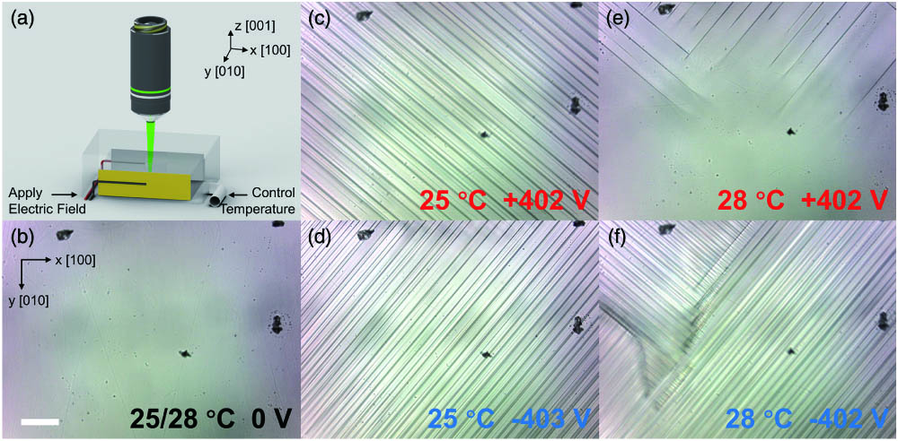
Figure 1.(a) Sketch of the experiment setup; coordinate axes are defined here. (b)–(f) Micrographs of the KTN sample under different conditions. (b) The sample in the single domain state at 25°C or 28°C. The sample in the multiple domain state (c), (d) at 25°C and (e), (f) at 28°C under positive/negative electric fields. The scale bar in (b) is 100 µm. The spots on the sample surface assure the measurement position to be the same.
3. Results and Discussions
During the process of paraelectric–ferroelectric phase transition, the ferroelectric domain structures are formed with sizes of several micrometers, which can be observed under an optical microscope. To minimize the free energy, the PNRs in the crystal tend to form the standard perovskite 90° ferroelectric domain structures with an appearance of 45° ferroelectric domain walls. However, after a long period of relaxation ( week), the ferroelectric domains are merged into new larger domains. The crystal will eventually become one whole ferroelectric domain, a single domain state, as displayed in Fig. 1(b).
When the sample is placed in an electric field (), we observe that the crystal undergoes a transformation from its single ferroelectric domain to multiple ferroelectric domains immediately, as illustrated in Figs. 1(c)–1(f). The domain boundaries formed under the positive electric field are aligned perpendicularly to those under the negative electric fields. At 25°C, the domain boundaries are quasi-periodically aligned along the same direction since the ferroelectric domains distribute evenly. However, the inhomogeneity of the ferroelectric domains appears at 28°C, which is close to the Curie temperature of the sample. Therefore, this phenomenon can be ascribed to the relaxation properties of the KTN crystal. The demarcation lines of the orthometric domain boundaries in Figs. 1(e) and 1(f) demonstrate the existence of defects or local component inhomogeneity in this region. Therewith, in the critical state at 28°C, PNRs induced by the local inhomogeneity can emerge at the earliest. These dynamic ferroelectric microstructures present relatively weak interactions with the external electric field. Therefore, a large number of PNRs can block the external electric field locally, leaving an untransformed single domain or transformed multiple domains but with different polarization directions with the external electric field. In this sense, the differences of the Figs. 1(e) and 1(f) are because the PNRs formed in the inhomogeneous regions block the external electric field in different regions under the electric fields with different directions.
To further understand the crystalline differences between the single domain state and the multiple domain state, Raman spectrum measurements are implemented, and the results are shown in Fig. 2. There are several typical vibrational modes in the Raman spectrum of KTN crystal, including the second-order transverse acoustic (2TA) mode at , which is induced by two transverse acoustic (TA) phonons at the Brillouin zone boundary, the modes at (i.e., the peak of the Fano resonance), which represent the relative motion between the ions and the frameworks of the octahedral units, and the modes at and the modes at , which correspond to the deformation of the frameworks.
![]()
Figure 2.Raman spectra of the KTN sample (a) at 25°C and (c) at 28°C under zero/positive/negative electric fields. The enlarged Raman spectra around the TO3 modes corresponding to the temperatures of (b) 25°C and (d) 28°C.
Under electric fields, the vibrational modes, 2TA, , and , are strongly suppressed [Figs. 2(a) and 2(b)], while the mode is further enhanced [Figs. 2(c) and 2(d)], compared to that in the absence of the electric field. The suppression of the 2TA mode can be ascribed to the distortion of the Brillouin zone in the multiple domain state. The intensity decrement of the modes represents the suppression of the relative motions between the ions and the frameworks of the octahedral units. On the other hand, the intensity decrement of the modes represents the suppression of the relative motions of the ions, which belong to different atom layers inside the frameworks. Besides, the enhancement of the modes is caused by the increasing motions of the in-layer ions inside the frameworks. This phenomenon is in good agreement with the inference that in the multiple domain state the relative positions of the atom layers are “locked” to each other in the domain boundaries, causing the interlamination relative motions to be restricted.
Correspondingly, the in-layer vibrational modes are further enhanced because of the conservation of internal energy. There should be no differences between the positive and negative electric field conditions if the sample is strictly homogeneous. However, the KTN crystal is an incongruent material with its composition varied gradually along the crystal growth direction (i.e., the direction). In the multiple domain ferroelectric state, this inhomogeneity will extend to the other two dimensions by the 90° ferroelectric domain structures. Therefore, the sample in the multiple domain ferroelectric state presents a slight intensity difference in the Raman spectra under electric fields with different directions.
The relative permittivity variations also confirm the transformation from the single domain state to the multiple domain state under electric field, as shown in Fig. 3. Both the single domain state before the transition and the multiple domain state after the transition present relatively stable ferroelectric domain structures with an ability to resist external electric fields. Therefore, a relative permittivity peak that represents the transformation will be formed as the electric field intensity increases. In comparison, the unstable ferroelectric domain structures formed during the transformation process are much more sensitive to the external alternating electric field. Also, the difference of the coercive electric fields (defined as the electric field value at the relative permittivity peak) between the positive and negative electric fields at 25°C can also be ascribed to the inhomogeneity of the sample. At 28°C, the difference of the coercive electric fields decreases since the formation of PNRs introduces dynamic polarization and protects several regions from the external electric field. In addition, the double peaks of the relative permittivity under a positive electric field also demonstrate the blocking effect of PNRs.
![]()
Figure 3.Relative permittivity varying with increasing electric field of the KTN sample (a) at 25°C and (b) at 28°C under positive and negative electric fields.
For a better understanding of the related mechanisms, we establish an intuitive model to visualize the field-induced transformation process of ferroelectric domains, as illustrated in Fig. 4. A single domain state will emerge spontaneously with a long-period relaxation after the sample completes a paraelectric–ferroelectric phase transition. Besides, most of the ferroelectric domains tend to reorientate along the composition gradient direction. When the sample is in the single domain state, the single ferroelectric domain has its polarization aligned to the same direction, as shown in Fig. 4(a).
![]()
Figure 4.Diagram of the field-induced transition process from the single domain state to the multiple domain state. (a) Sample in the single domain state. (b) Under a relatively low electric field, the state transition begins. (c) Under a relatively high electric field, the polarization of the field-induced ferroelectric domain can bear comparison with the polarization of the spontaneous ferroelectric domain; as a result, domain boundaries form. (d) Under the reversed electric field, the domain boundaries rotate 90°.
However, when the sample is placed in an electric field of which the intensity can conquer the spontaneous polarization of the original ferroelectric domain, the single domain breaks down into multiple ones with the polarization along the external electric field, forming a 90° ferroelectric domain structure (i.e., 45° ferroelectric domain boundary), as displayed in Figs. 4(b) and 4(c). In this case, only the head-to-tail domain boundaries can form because of the electric dipole-dipole interactions[
4. Conclusions
In conclusion, we have successfully implemented a unique field-induced state transformation of ferroelectric domains by using KTN crystal. By applying the electric field, the KTN sample transforms from its single domain state to the multiple domain state. Confocal µ-Raman measurement reveals the dynamic change of lattice structures induced by the external electric field. The result of the relative permittivity measurement also confirms this transformation. The use of the electric field enables feasibility to precisely manipulate the ferroelectric domain state. Our study facilitates not only a further understanding of the ferroelectric phase transition but also wide device applications by using the ferroelectric KTN crystal.
References
[1] X.-P. Wang, Q.-G. Li, Y.-G. Yang, Y.-Y. Zhang, X.-S. Lv, L. Wei, B. Liu, J.-H. Xu, L. Ma, J.-Y. Wang. Optical, dielectric and ferroelectric properties of KTa0.63Nb0.37O3 and Cu doped KTa0.63Nb0.37O3 single crystals. J. Mater. Sci. Mater. Electron., 27, 13075(2016).
[2] F. Huang, C. Hu, Z. Zhou, X. Meng, P. Tan, Y. Wang, C. Wang, H. Tian. Improving strain in single crystal by composition-gradients design. Acta Mater., 200, 24(2020).
[3] X. Li, Q. Yang, H. Liu, Y. Ren, X. Wang, P. Wu. UV-enhanced conductive and dielectric properties in KTN crystal. Ceram. Int., 47, 11989(2021).
[4] X. Li, Q. Yang, X. Zhang, S. He, X. Wang, H. Liu, P. Wu. High transparency induced by electric fields using KTN crystals. J. Alloys Compd., 842, 155702(2020).
[5] X. Zheng, H. Zhao, X. Wang, B. Liu, J. Yu, X. Zhao. Phase evolution and dielectric/ferroelectric properties of KTa0.67Nb0.33O3 single crystal. Ceram. Int., 41, S197(2015).
[6] Y. C. Chang, C. Wang, S. Yin, R. C. Hoffman, A. G. Mott. Giant electro-optic effect in nanodisordered KTN crystals. Opt. Lett., 38, 4574(2013).
[7] Q. Lu, B. Li, Z. Li, B. Ge. Field-induced lifetime enhancement of photorefractive gratings in a Mn:Fe:KTN crystal. Opt. Lett., 42, 2407(2017).
[8] X. Zhang, Q. Yang, H. Liu, X. Wang, S. He, X. Li, P. Wu. Switching effects of spontaneously formed superlattices in relaxor ferroelectrics. Opt. Mater. Express, 9, 4081(2019).
[9] Q. Yang, X. Zhang, H. Liu, X. Wang, Y. Ren, S. He, X. Li, P. Wu. Dynamic relaxation process of a 3D super crystal structure in a Cu:KTN crystal. Chin. Opt. Lett., 18, 021901(2020).
[10] F. Di Mei, L. Falsi, M. Flammini, D. Pierangeli, P. Di Porto, A. J. Agranat, E. DelRe. Giant broadband refraction in the visible in a ferroelectric perovskite. Nat. Photon., 12, 734(2018).
[11] Y. Wang, X. Meng, H. Tian, C. Hu, P. Xu, P. Tan, Z. Zhou. Dynamic evolution of polar regions in KTa0.56Nb0.44O3 near the para-ferroelectric phase transition. Cryst. Growth Des., 19, 1041(2019).
[12] X. Li, Q. Yang, X. Zhang, S. He, H. Liu, P. Wu. Heating-rate-dependent dielectric properties of KTa0.58Nb0.42O3 crystal in paraelectric phase. Cryst. Growth Des., 20, 2578(2020).
[13] P. Wu, X. Jiang, B. Zhang, S. He, Q. Yang, X. Li, Y. Ren, F. Chen, H. Liu. Mode-controllable waveguide fabricated by laser-induced phase transition in KTN. Opt. Express, 28, 25633(2020).
[14] X. Li, Q. Yang, X. Zhang, S. He, H. Liu, P. Wu. Low DC electric-field-induced phase transition in KTa0.59Nb0.41O3 crystal. Cryst. Growth Des., 20, 1248(2019).
[15] S. He, Z. Zhang, H. Liu, S. Akhmadaliev, S. Zhou, X. Wang, P. Wu. Spatial solitons in KTaxNb1-xO3 waveguides produced by swift carbon ion irradiation and femtosecond laser ablation. Appl. Phys. Express, 12, 076502(2019).
[16] S. He, Q. Yang, B. Zhang, Y. Ren, H. Liu, P. Wu, Y. Yao, F. Chen. A waveguide mode modulator based on femtosecond laser direct writing in KTN crystals. Results Phys., 18, 103307(2020).
[17] S. He, Q. Yang, X. Li, H. Liu, L. Cao, S. Akhmadaliev, X. Wang, Y. Ren, S. Zhou, P. Wu. Para-ferroelectric phase transition driven by swift heavy-ion irradiation in KTN crystal. Appl. Surf. Sci., 519, 146261(2020).
[18] V. Laur, A. Moussavou, G. Tanne, P. Laurent, V. Bouquet, S. Deputier, M. Guilloux-Viry, F. Huret. Reconfigurable circuits for wireless applications using KTN ferroelectrics. 2007 European Microwave Conference, 102(2007).
[19] X. Meng, H. Tian, C. Hu, J. Yang, L. Li, B. Yang, Z. Zhou. Elastic, piezoelectric, and dielectric properties of high-quality KTa0.53Nb0.47O3 single crystal with tetragonal phase. J. Alloys Compd., 773, 21(2019).
[20] W. Haas, R. Johannes. Linear electrooptic effect in potassium tantalate niobate crystals. Appl. Opt., 6, 2007(1967).
[21] S. Loheide, H. Hesse, E. Krätzig, K. H. Ringhofer. Photorefractive properties of tetragonal potassium tantalate-niobate crystals. Opt. Mater., 2, 65(1993).
[22] S. Riehemann, D. Sabbert, S. Loheide, F. Matthes, G. von Bally, E. Krätzig. Holographic double-exposure interferometry with tetragonal KTa1−xNbxO3:Fe crystals. Opt. Mater., 4, 437(1995).
[23] F. Huang, C. Hu, Z. Xian, X. Sun, Z. Zhou, X. Meng, P. Tan, Y. Zhang, X. Huang, Y. Wang, H. Tian. Photovoltaic properties in an orthorhombic Fe doped KTN single crystal. Opt. Express, 28, 34754(2020).
[24] X. Cao, H. Tian, C. Hu, Y. Wang, X. Li, L. Li, X. Sun, Z. Zhou. Discovery and evolution of double P-E loops in a tetragonal Fe-doped KTa0.57Nb0.43O3 single crystal. J. Am. Ceram. Soc., 101, 3755(2018).
[25] P. Zhang, D. Liu, A. Yang, J. Zhu. Optimization of compensation for high spatial frequency in distorted wavefront using optical phase conjugation. Chin. Opt. Lett., 17, 070901(2019).
[26] Y. Niu, L. Yang, D. Guo, Y. Chen, X. Li, G. Zhao, X. Hu. Efficient 671 nm red light generation in annealed proton-exchanged periodically poled LiNbO3 waveguides. Chin. Opt. Lett., 18, 111902(2020).
[27] C. Qiu, B. Wang, N. Zhang, S. Zhang, J. Liu, D. Walker, Y. Wang, H. Tian, T. R. Shrout, Z. Xu, L. Q. Chen, F. Li. Transparent ferroelectric crystals with ultrahigh piezoelectricity. Nature, 577, 350(2020).
[28] X. Wang, J. Wang, Y. Yu, H. Zhang, R. I. Boughton. Growth of cubic KTa1−xNbxO3 crystal by Czochralski method. J. Cryst. Growth, 293, 398(2006).
[29] H.-L. Hu, L.-Q. Chen. Three-dimensional computer simulation of ferroelectric domain formation. J. Am. Ceram. Soc., 81, 492(1998).
[30] Y. Ishibashi, E. Salje. A theory of ferroelectric 90 degree domain wall. J. Phys. Soc. Jpn., 71, 2800(2002).

Set citation alerts for the article
Please enter your email address
© Copyright 2018-2021 | Chinese Laser Press. All Rights Reserved 沪ICP备15018463号-20