In this Letter, we fabricate integrated metasurface of encoded dynamic phases and experimentally generate nonconventional Kagome-type lattices of no-second-order phase vortices. The thin metasurface acts analogous to an integration of three conventional optical elements, i.e., six pinholes located at the vertices of two concentric regular triangles of size ratio 1:2, six transparent discs of different thicknesses to introduce a total phase shift difference of , and a Fourier lens with a focal length in the micro-scale. A Kagome lattice with the required vortex distribution is realized at the “focal” plane of the metasurface under illumination of the plane wave.
A Kagome lattice is a pervasive pattern in nature, and its full view looks like isolated dark areas enclosed in triangles and hexagons, as described by the sense of the word “hole in the basket”; in detail, triangles sharing one vertex point with neighbors and six such shared vertex points forming a hexagon[1]. The band structure of a two-dimensional Kagome lattice has dispersionless flatbands, and ferromagnetism appears when the flatbands are half filled, making it possible to realize super-solidity for scalar bosons, ferromagnetism of itinerant fermions, and topological phases, since inter-partical interactions play a prominent role in these fields[2–4]. When atoms and molecules are trapped by optical Kagome lattice structures, they show many intriguing behaviors such as Mott insulators of bosons and fermions[5,6]. Due to these intriguing properties, the Kagome lattice has attracted considerable concentration in simulating many-body physics condensed-matter and topological insulators[7,8]. Mentioning matter structuring, a Kagome lattice is also useful for its convenience to optically induce photonic lattices in photorefractive crystals or tweeze particles for self-assembly[9].
No matter how many theoretical analyses or applications on Kagome lattices have been conducted, their further developments and applied ability are closely dependent on the experimental realization. Up to now, researchers have proposed many experimental methods on this issue[10]. The most known ones include self-assembly[11] and optical interference. The latter one is undoubtedly advantageous for its convenience to manipulate both the sizes and detailed patterns of the generated lattices. In literature, Kagome-type light fields, as well as other types of optical lattices, have been realized by overlapping two commensurate triangular optical lattices with 532 nm and 1064 nm wavelengths[5], combining a computer-controlled spatial light modulator and Fourier filter systems[12], precisely arranging six ablated gratings or pinholes in in-plane radial directions[13,14], just to mention a few. However, the vortex arrays embedded in the lattices are in the same form, i.e., first-order vortices within the triangles and second-order vortices within the hexagons[10]. New types of Kagome lattices with different embedded vortex arrays may enhance or enlarge their applications in phase-related fields such as optical communication, super-resolution structure inducing, and optical spanner[15].
In this Letter, we propose an experimental method for generating Kagome-type lattices with no second-order vortices embedded. The corresponding optical scheme can be illustrated as the Fourier transform of six parallel light beams with both pre-determined spatial positions and pre-given phase variations between neighboring ones. However, from the perspective of experiment, the adjustment of the optical setup for realizing such a scheme may be too complex, and the optical elements used may be too large to be integrated into multifunctional systems. This common drawback of experimental setups hampers Kagome lattices, as well as other types of optical lattices, to be applied in micro- or nano-scale fields.
Sign up for Chinese Optics Letters TOC. Get the latest issue of Chinese Optics Letters delivered right to you!Sign up now
The metasurface has also attracted great attention due to its ability in optical shaping[16–20]. By tuning the positions, sizes, and shapes of the nanostructures on the metasurface, one can readily modulate the amplitudes, phases, and polarizations of the light waves transmitting through or reflected from the metasurface[21–23]. Such modulation is the essential role that many optical elements, e.g., phase retarders and lenses, play in an experimental setup[24]. It provides a feasible method to generate a Kagome lattice by realizing the above generation mechanism using a designed metasurface. In detail, the six parallel laser beams can be realized by arranging the nanostructures in six circular areas with designed in-plane positions to lead the incident laser beam transmitting from them. Both the phase differences between the six transmitting waves (dynamic phase) and the spherical phase profile corresponding to a Fourier lens (propagating phase) can be simultaneously obtained due to the spin-orbital interaction[25,26] by the designed nanostructures (geometric phases). In other words, the metasurface may be regarded as an upgraded pinhole interferometer integrating a six-pinhole plate and a Fourier lens together. This provides a simple way for fabricating thin and integrated optical elements to experimentally generate unconventional Kagome-type lattices, which has potential applications in a diversity of fields such as near-field optical micro-manipulation and micro-lithography.
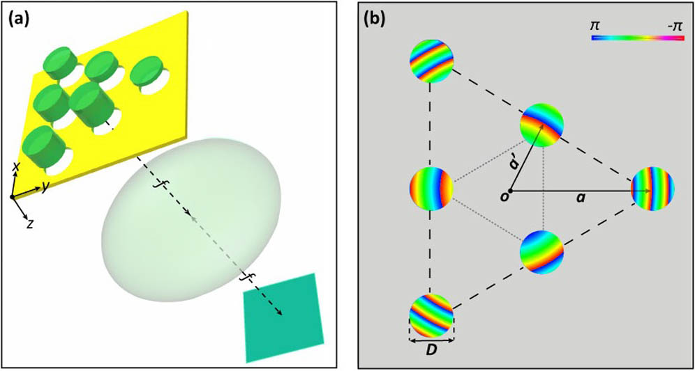
Figure 1 depicts the generation scheme. The six-pinhole plate is composed by two regular three-pinhole interferometers, which have a size ratio of 2:1, and the two constituent ones are concentrically combined together with an azimuthal rotation angle of sixty degrees. The six pinholes have an identical size, and this ensures that the waves from them have the same amplitude. At each of the pinholes, a transparent thin disc is mounted, see Fig. 1(a). The disc at the pinhole with a larger azimuthal angle is thicker, and the total optical path difference between the six discs is triple the wavelength of the illuminating wave. Thus, the multiple transmitting waves from the pinholes are imposed of a total phase delay of . These waves impact upon a Fourier lens, the pinhole plate is placed at its focal plane, and the waves interfere with each other at the back focal plane of the lens. A Kagome-type lattice with the required phase distribution is expected to appear at the interference field.
Figure 1.Schematic diagram for generating novel Kagome lattices. (a) Conventional setup may be composed by six pinholes, six transparent discs, and a lens with focal length . The functional effect of their combination can be integrated into a single plane (b) with both amplitude modulation and phase modulation.
As mentioned above, the six pinholes, the transparent discs, and the Fourier lens can all be combined onto a single metasurface film by encoding both amplitude modulation and phase modulation. The pinholes are simply represented by six spatially arranged circular areas in this film, and the amplitude transmission function of the th circular area is given as where is the point position in the metasurface film, is the center position of the th circular area, is the distance from the pinhole centers to the plate origin, represents the transmittance function of the circular area with as its radius, and is the remainder function. The six discs and the Fourier lens are essentially phase-only modulators, and they are represented as phase values (dynamic phase and propagating phase). In detail, the relative phase shifts induced by the discs are at the th pinhole, and the Fourier lens introduces a spherical phase retardation profile. For a lens with focal length of , the phase retardation profile can be expressed as where is the absolute wave vector of the illuminating wave with wavelength . Then, the total modulation, including amplitude and phase, of the metasurface film can be written as
For intuitive observation, the modulation of the metasurface film is schematically depicted in Fig. 1(b).
According to previous studies, metasurfaces may be realized by using optically thin films made of lossy or material arrays of optical scatterers[27]. Considering that the metasurface in our present work should be opaque except for the circular pinhole areas, we choose 200 nm thick gold film on a 5 mm thick quartz substrate as the metasurface base, as shown in Fig. 2. On the gold film, we drill arrays of nano-apertures using a focused ion beam (FIB) etcher, where these nano-apertures are localized into six circular areas corresponding to the six pinholes in Fig. 1(a). These nano-apertures are in length and in width, and the distances between neighboring nano-aperture centers are in both and directions, as shown in Fig. 2(a). According to the spin–orbit interaction, a nano-aperture with a size smaller than wavelength (532 nm in our experiment) performs analogous to a polarization filter, where only the polarization component perpendicular to the long side of the aperture could pass through. By azimuthally rotating the nano-aperture, phase retardation (geometric phase) ranging from 0 to can be readily obtained under circular polarization illumination, i.e., under left- or right-handed circular polarization, where is the aperture’s orient angle rotation with respect to a referenced nano-aperture[27,28]. Here, in this Letter, the nano-aperture with the long side lying along the direction is set as the reference aperture, and the transmitting wave from it is regarded to be with zero phase retardation under left-handed circular polarization. Moreover, it has been verified that the amplitude transmittance for all rotating angles is the same, ensuring the identical wave amplitude from the apertures[29,30]. So, by precisely rotating the nano-apertures to satisfy the required geometric phase retardation value at their centers, we obtain the dynamic wave modulation of Eq. (3) on the metasurface, see Fig. 2(b). Likewise, Eq. (3) can alternatively be realized under right-handed circular polarization by rotating the nano-apertures in an opposite azimuthal direction. Then, as the transmitted waves propagate and interfere with each other, the required Kagome-type lattice can be generated at the designed focal plane of the metasurface. The scanning electron microscope (SEM) image of the designed metasurface film is shown in Fig. 2(c). Herein, the focal length of the Fourier lens is set as , the pinhole diameter is , and the distances from the pinholes to the film center are and , respectively.
Figure 2.(a) Schematic of the phase modulation using the metasurface of nano-apertures. The thickness of the gold film on the quartz substrate is 200 nm. For each nano-aperture, the length of each is , the width is , and the distance between neighboring apertures is 220 μm in both the and directions. Tuning the oriented angle difference between two apertures, we can realize a certain phase shift of in their transmitted waves. (b) Full image of the designed metasurface corresponding to Fig. 1(b). (c) SEM image of the fabricated metasurface.
The 532 nm single-mode laser from a solid laser is used to illuminate the fabricated metasurface with normal incidence. To obtain left-handed circular polarization, the input laser first passes through a polarizer and then a quarter-wave plate before reaching the metasurface. A combination of a complementary metal–oxide–semiconductor (CMOS) and a objective lens with numerical aperture of 0.9 is placed behind the metasurface to magnify and record the interference wave field of the transmitting waves. For readily adjusting the distance between the objective lens and the metasurface, the metasurface is mounted on a nano-positioning stage. We also introduce a reference beam to interfere with the interference wave field. From the interferogram, one could intuitively see where a phase exists and of what topological charge it is.
The generated intensity pattern and its interferogram with the reference beam, both recorded by the CMOS at the “focal plane” of the metasurface, are shown in Figs. 3(a) and 3(b), respectively. As marked by the red contour lines in Fig. 3(a), this intensity pattern could be characterized as periodic patchwork of hexagonal spot unit arrays and hourglass arrays consisting of five intensity maximums. Obviously, such an intensity pattern obeys the Kagome-type distribution. We see from Fig. 3(b) that one interferometric fringe splits into two at the dark point within those hourglasses. This indicates the generation of a first-order phase vortex there. What is not reported in previous studies is that there no splitting of interferometric fringes within those hexagonal spot units exists, or in other words, no phase vortex is generated.
Figure 3.(a) Intensity distribution recorded by the CMOS. The intensity pattern is a periodic patchwork of hexagonal spot unit arrays and hourglass arrays consisting of five intensity maximums, as marked by red lines. (b) Interferogram of (a) and the reference wave. An interference fringe splits into two within the hourglass, but no splitting is seen within the hexagon.
Obviously, a Kagome-type lattice with conventional phase distribution can also be generated using the proposed metasurface scheme. According to the demonstrations in previous studies, the six pinholes should be located at the vertices of a regular hexagon, and the total phase shift induced by different disc thicknesses should be . The generated intensity pattern therein is nearly the same as in Fig. 3(a). But, the phase within the dark area in the hexagonal spot unit has a progressive increment of , indicating a second-order phase vortex.
Similar with other optical interferometric mechanisms, the size of the generated Kagome lattice is closely related with the design parameters of the metasurface. Obviously, the Kagome lattice is the Fourier transform of the transmitting waves from the metasurface. Its whole area is proportional to , and its lattice period , defined as the distance between neighboring hexagonal spot units, can be written as
In this Letter, such a lattice period is calculated to be 4.5 μm.
In fact, the nano-apertures are not the full representation of Fig. 1(b) but sampled points. As a result, the generating Kagome lattice does not take full use of the incident wave power. One method for improving the quality of the generated lattice and increasing the energy coefficient is to appropriately decrease the sampling interval by using smaller nano-apertures and aperture distances, as long as the apertures are not so close to induce crosstalk. Another method is to enlarge both the circular area and their distances to let more illuminating waves pass through. This method requires an excellent FIB fabrication technique.
According to the simulations in Ref. [31], a Kagome-type lattice without a second-order phase vortex can also be obtained if we decrease the thickness differences between the transparent discs in Fig. 1(a), which takes effect via inducing a smaller pre-given phase difference of between the six transmitting waves. The resultant wave field is expected to be the same as in Fig. 3.
Alternatively, we also experimentally realize the scheme of Fig. 1(a) by conventional means, using a spiral phase plate to replace the six transparent discs. Six pinholes are drilled onto commercial oven-used aluminum foil by a femtosecond laser. The pinhole diameters are identically 20 μm to ensure the same amplitudes of the transmitted waves. The radial distances from the interferometer origin to the two constituent ones are and , respectively. The spiral phase plate is of a unity topological charge, corresponding to the incident light wavelength of 532.8 nm. It is coaxially placed closely in front of the six-pinhole plate to provide the transmitting waves with a progressively increasing pre-given phase difference. The focal length of the Fourier lens we used to generate the optical Kagome lattice is . Then, the generated wave field, at the focal plane of the Fourier lens, is directly recorded by the CMOS, as shown in the left panel of Fig. 4. Obviously, the intensity pattern is of a Kagome type. Due to the large size ratio of (and ) to pinhole diameter, we can see a much larger number of Kagome patterns. Its interferogram with a tilted plane wave is shown in the right panel of Fig. 4. Similar with that in Fig. 3(b), no fringe splitting could be obviously seen within the hexagonal spot units. A corresponding phase distribution type can be referred to the simulation results in Ref. [31].
Figure 4.(a) Kagome lattice generated after a six-pinhole interferometer. (b) Interferogram of (a) with a tilted plane wave.
In conclusion, a nonconventional Kagome-type lattice without second-order phase vortices is experimentally generated using a metasurface that is essentially a functional integration of a Fourier lens and a unique six-pinhole interferometer. The six circular areas on a thin light gold metasurface are located at the vertices of two concentric regular triangles of size ratio 1:2, modulating the amplitude of transmitting waves. A pre-given phase variation of in total and the spherical phase profile induced by a Fourier lens are all integrated together and encoded onto the metasurface by positioning and rotating punched nano-apertures on it. Under illumination of the plane wave of circular polarization, the interaction between light and nano-apertures induces geometric phases that lead to the decoding of the encoded dynamic phase profile. As the transmitted waves propagate and interfere with each other, a Kagome lattice is realized at the designed focal plane of the integrated metasurface. What is interesting and nonconventional is that only first-order phase vortex arrays, but not second-order phase vortices, are embedded in the generated lattice. Such kinds of a Kagome-type lattice may behave in a much different way in application field related to optical lattices. Moreover, this work confirms the transformation from the geometric phase to the dynamic phase and provides a tool to generate many other types of lattices or phase vortex arrays that can be realized by interference.