Yaoran Liu, Zilong Wu, Eric H. Hill, Yuebing Zheng. Mid-infrared superabsorbers based on quasi-periodic moiré metasurfaces[J]. Chinese Optics Letters, 2018, 16(5): 050004
Copy Citation Text
We report on mid-infrared superabsorbers based on quasi-periodic moiré metasurfaces in metal-insulator-metal form. By varying the spacer thickness, moiré rotation angle, and filling factor of the superabsorbers, we can tune narrowband or broadband absorption in a systematic way. With their high tunability of near-unity absorption and simple fabrication, in combination with decoupled mode theory for an efficient design, moiré superabsorbers are well-suited for a wide range of applications in sensing, imaging, and communication.
Mid-infrared (MIR) absorbers have attracted great interest for applications in sensing, thermal detection, and communication [1]. A type of MIR superabsorber of recent interest is based on plasmonic nanostructures[2–6] and a metal film with an insulator thin film between them, abbreviated as metal-insulator-metal (MIM)[7–11]. Plasmon-enhanced wave absorption and scattering, in combination with multiple reflections in MIM, enables near-unity narrowband[12,13] and broadband[14–16] MIR superabsorbers. So far, MIM superabsorbers have been mostly based on periodic[17,18] or random[19] arrays of plasmonic nanostructures. Compared with periodic or random arrays, quasi-periodic arrays of variable nanostructures have a higher tunability of spatial-frequency densities, and thus richer Fourier spectra. Therefore, quasi-periodic nanostructures are important for the development of broadband or multiband wave applications[20,21]. Quasi-periodic photonic crystals with Fibonacci sequence[22], Thue–Morse[23], and Rudin–Shapiro patterns[24] have been demonstrated. However, due to a lack of deterministic unit cells, large-scale quasi-periodic arrays of precisely controllable properties have remained challenging for simulation and fabrication.
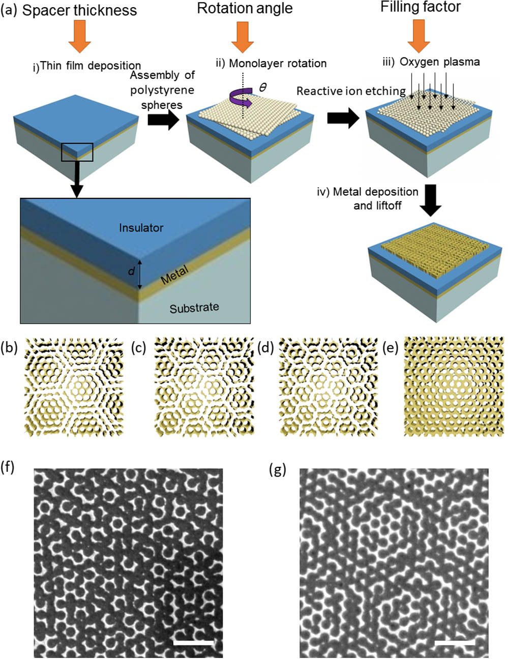
Here, an analytical approach is carried out to calculate and simulate the performance of moiré metasurfaces in MIM form toward developing high-performance MIR superabsorbers. Specifically, recently developed moiré nanosphere lithography (MNSL)[25–27] enabled high-throughput, low-cost fabrication of moiré metasurfaces. As shown in Fig. 1(a), systematic tuning of the moiré superabsorbers is made possible by controlling spacer thickness, rotation angle, and filling factor of the MIM moiré structures. Figures. 1(b)–1(e) show various moiré metasurfaces with different rotation angles. Figures 1(f) and 1(g) show the scanning electron micrograph of a fabricated Au moiré metasurface.
Figure 1.(a) Fabrication procedure of MIM moiré superabsorbers with variable parameters (i.e., spacer thickness d, rotation angle , and filling factor). (b)-(d) Moiré metasurfaces with variable rotation angles of 10°, 15°, and 20°, respectively. (e) 20° moiré metasurface with a higher filling factor than that in (d). (f), (g) Scanning electron micrographs of Au moiré metasurfaces. The scale bar is 2 μm.
Among various quasi-periodic structures[20,21], moiré patterns have a relatively high rotational[28,29] and translational symmetry[30]. For moiré patterns fabricated by MNSL[25], six-fold rotational symmetry exists for all rotational angles. Here, a method to find the unit cell in a quasi-periodic moiré pattern is proposed in order to simplify simulation. Two sets of unit vectors , and , are defined in a hexagonal hole array, shown in Fig. 2(a), where is the lattice constant of the array. Based on these unit vectors, vector is specified as and vector is specified as . Figure 2(b) shows an area using and . Here, and are chosen to satisfy is defined as the rotation angle of the second nanosphere array relative to the first nanosphere array, where is chosen as an example. By using the previously defined area and applying the same area to the top nanohole array with a relative 15° rotation angle, shown in Fig. 2(c), the unit cell of the moiré pattern can be defined as the overlapping regions of the top and bottom nanohole arrays within this rectangular area shown in Fig. 2(d). This method can be applied to any rotation angle of a moiré pattern by choosing the appropriate and . However, it will increase the computation time once and are very large for a specific angle. To reduce and , but still apply the above method to find the unit cell, we set as a tolerance factor, which is defined as the difference between the right-hand side (RHS) and the left-hand side (LHS) of the above Eqs. (1) and (2). Then, the above equations can be modified as
Sign up for Chinese Optics Letters TOC. Get the latest issue of Chinese Optics Letters delivered right to you!Sign up now
Figure 2.(a) Unit vectors in the hexagonal hole array. (b) A rectangular area in the hexagonal hole array using and as the length and width separately. (c) The same area as (b) but with a relative rotation angle. (d) A unit cell in the moiré pattern with a relative rotation angle. (e) A unit cell for 10°, 15°, and 20° moiré metasurfaces.
By setting to find the chosen and with a minimum of , Table 1 shows the calculated and values for different tolerance factors when the rotation angle is 15°. As and increase, δ will become smaller so that RHS and LHS in Eqs. (3) and (4) become approximately equal, which can be regarded as the real moiré pattern.
Rotation Angle
Tolerance
m
m′
n
n′
15°
δ=0.1
1
1
1
5
15°
δ=0.01
5
1
8
6
15°
δ=0.001
17
11
27
67
Table 1. m, m′, n, and n′ Values for Different Tolerance Factors as θ Equals 15°
However, there is a trade-off between the simulation accuracy and simulation efficiency as varies. A small will increase the simulation accuracy but reduce the computational efficiency. An optimized will ensure that the error of this continuity is still within the simulation mesh resolution. is chosen to generate unit cells for three rotation angles (10°, 15°, and 20°) shown in Fig. 2(e). Here, the lattice constant is set as 300 nm. Diameters of the bottom hole and top hole are set to 250 nm and 150 nm separately, where the chosen and values are shown in Table 2.
Rotation Angle
Tolerance
m
m′
n
n′
10°
δ=0.01
3
2
4
19
15°
δ=0.01
5
1
8
6
20°
δ=0.01
6
2
11
9
Table 2. m, m′, n, and n′ Values Used in Simulation for Different Rotation Angles
After simplifying the quasi-periodic pattern as a continuous periodic pattern with a unit cell, the following theory behind the simulations is based on a traditional periodic metasurface. Decoupled mode theory has been frequently used in studying superabsorbers based on periodic metasurfaces in MIM form[31]. This approach reduces the simulation time while revealing the physical resonance mechanism of the superabsorbers. It does not consider any near-field interactions or magnetic field when the spacer thickness is large enough compared with the top metal film.
Here, we also apply decoupled mode theory to design moiré MIM structure as follows. A metasurface is placed at the interface between the air and a dielectric spacer, which acts as a partially reflective surface shown in Fig. 3(a). The thickness of the metasurface is chosen as 10 nm based on a previous MIR absorber design[17]. The amplitude and phase of the incident light between the air and a dielectric spacer will change due to the perturbation of the metasurface. Suppose that incident light from air approaches the air/metasurface interface with a unity amplitude. It is partially reflected with and partially transmitted into the dielectric spacer with . After a bounce path from the ground plane with phase change, light from the dielectric spacer returns. Like before, this returning light can also be divided into reflected light with a reflection coefficient and transmitted light with a transmission coefficient at the air/metasurface interface. Here, the moiré metasurfaces perturb the amplitude and phase of the incident light. Thus, we can calculate the amplitude () and phase () coefficients separately for different moiré metasurfaces with incident light, as shown in Fig. 3(b). As an example, Fig. 3(c) shows the simulated reflection and transmission coefficients for a 15° moiré metasurface using a unit cell, shown in Fig. 2(d). By using the simulated amplitude and phase coefficients of a pristine moiré metasurface, the superposition of multireflection within the spacer can be written as
Figure 3.(a) Cross-sectional view of , , , and in decoupled mode theory. (b) The simulation model to calculate the parameters , , , and . (c) The simulated reflection/transmission phase and amplitude coefficients for a 15° rotation angle moiré metasurface.
Since the transmission through the bottom metal layer is zero, the total absorption of this configuration can be written as
Therefore, the absorption for different spacer thicknesses can be calculated for different moiré patterns. shown as a solid line in Figs. 4(a) and 4(b). Here, the refractive index of the dielectric layer remains constant at 1.377.
Figure 4.(a) Simulated (black dashed line) absorption for a 15° rotation angle pristine (no spacer) moiré metasurface; simulated (dashed red and blue line) and calculated (solid black line) results comparison for a 15° rotation angle moiré MIM structure with 800 nm spacer thickness. The PML boundary is applied in the simulation. (b) Simulated (dashed line) and calculated (solid line) results comparison for different rotation angles at 800 nm spacer thickness. The periodic boundary is applied in the simulation.
To verify the quasi-periodic unit cell model, we use a perfectly matched layer (PML) boundary and simulate the whole MIM structure with the randomly chosen finite area. As an example, we simulate 10 μm and 30 μm size 15° quasi-periodic moiré MIM structures with a 800 nm spacer, shown as the red and blue dashed lines in Fig. 4(a). First, both show the same trend in the calculated result. The peak positions are almost the same for both the calculated results and simulated results. Second, the absorption increases with the simulation area. Even larger areas were not simulated due to the finite simulation resources using fine mesh. However, the simulations predict that the absorption will become even higher as the simulation area continues to increase, with almost perfect absorption as the calculated results assume an infinite area.
To verify decoupled mode theory, periodic boundaries and previous calculated unit cells are used to simulate the whole MIM structure. The dashed lines in Fig. 4(b) show a good agreement between the calculated results and simulated results for different rotations of MIM structure with the same thickness. Here, we choose the unit cell as Fig. 2(e). The nearly perfect match between the simulation and calculation results means that the near-field interaction and magnetic resonance contributes little to the absorption in this type of MIM superabsorber, which is a prerequisite to the use of decoupled mode theory. The enhanced absorption is mainly caused by the destructive superposition of multiple reflections and absorptions between the top moiré metasurface and the bottom metal layer.
To better understand the broadband absorption mechanism, we examine the absorption coefficient of a pristine moiré pattern (no spacer), shown as the dashed black line in Fig. 4(a). Strong absorption is observed from 3 μm to 6 μm. For other MIR ranges, the pristine moiré pattern also shows absorption above 20%. Such a range of MIR absorption shows the system’s potential for broadband superabsorbers. It was previously shown that moiré patterns have various sizes of split rings, -shaped, and fan-like nanostructures that support different orders of localized surface plasmon modes[26]. The nanogaps between these various nanostructures cause strong near-field coupling and lead to strong electric field enhancement. Due to the internal loss of metal and these various “hot spots”, this type of metasurface shows multiband absorptions. By applying an MIM configuration here, the absorption of pristine moiré patterns can be significantly increased.
The quasi-periodic unit cell model and decoupled mode theory pave the way to exploring versatile designs of moiré patterns. After optimizing the spacer thickness, Fig. 5(a) shows the calculated absorption of moiré MIM structures with higher filling factors, where we keep the same lattice constant as before but change the diameter of the bottom hole and top hole as 200 nm and 100 nm separately. Instead of broadband absorption, narrowband absorption with near-unity can be achieved. The overall structure in this case can be regarded as a thin metal hole array inserted between air and the dielectric spacer, which is typically shown as a narrowband absorption[32,33]. The diameters of the holes in the array and the thickness of the spacer greatly affect the resonance peak of the narrowband absorber. Compared with a low filling factor moiré pattern, it lacks various sizes of nanostructures, which limits its broadband resonances in a large range of the MIR.
Figure 5.(a) Calculated narrowband absorber with an optimized spacer thickness (1300 nm) at different rotation angles. (b) A calculated broadband absorber with an optimized spacer thickness (900 nm spacer for 10°, 800 nm spacer for 15°, and 700 nm spacer for 20°).
Figure 5(b) shows the calculated absorption of a moiré MIM structure with a lower filling factor after optimizing the spacer thickness. Moiré MIM structures with three rotation angles (10°, 15°, 20°) are examined. All show broadband absorption, with over 70% from 2.5 μm to 8 μm. However, there are a few differences in absorption, such as absorption range. The 10° MIM absorber shows a much broader absorption range, out to nearly 10 μm. It has been found that the absorption broadening depends on the size of the nanostructure[34]. Typically, longer strips or a larger continuous hole array will cause the wavelength to redshift, where smaller features lead to a blueshift. Here, the 10° MIM absorber has an increased size inhomogeneity of nanostructures, especially larger continuous nanostructures, compared with the 15° and 20° MIM absorbers. Thus, the 10° moiré MIM absorber shows much broader absorption.
To carry out polarization-dependent absorption analysis of the MIR absorbers, polarization dependence of broadband and narrowband absorption was calculated for a 20° moiré pattern, with the optimized spacer as an example. The results are shown in Fig. 6. The reason for uniform absorption under such a wide range of polarization angles is due to the quasi-hexagonal or quasi-triangular symmetry of the moiré pattern in the plane. This polarization-independent absorption demonstrates a high absorption under unpolarized light conditions.
Figure 6.(a) Simulated polarization-dependent broadband absorption for a 20° moiré MIM structure with an optimized spacer thickness. (b) Simulated polarization-dependent narrowband absorption for a 20° moiré MIM structure with an optimized spacer thickness.
It is worth noting that moiré MIM structures can also be designed to work in visible and near infrared (NIR) regimes. As an example, Fig. 7 shows simulated absorption spectra of the various 10° moiré MIM structures. We can see that the maximum absorption for the range from visible to NIR can be tuned by the spacer thickness in the MIM structures.
Figure 7.Simulated visible-NIR absorption spectra of a 10° moiré MIM structure with different spacer thicknesses.
In conclusion, the design rules for both narrowband and broadband quasi-periodic superabsorbers in MIR were determined through both theoretical calculations and simulations. The calculations agree well with the simulation results. Predicting the super-absorption performances of moiré MIM structures using a quasi-periodic unit cell model and decoupled mode theory required no computational optimization for spacer thickness. Our design rules are applicable for a variety of moiré patterns that work in the various spectral regimes. Compared with traditional quasi-MIM absorber design, our self-assembled moiré superabsorbers greatly reduce the fabrication cost. Our ability to efficiently model these absorbers prior to their fabrication will lead to optimum performances. These moiré superabsorbers are excellent candidates for surface-enhanced spectroscopy in molecular analysis[35]. They can also work as selective thermal emitters at the MIR for security imaging applications[36,37]. In addition, the moiré metasurfaces can be integrated with optoelectronic components for MIR telecommunication[8].
References
[1] S. Law, V. Podolskiy, D. Wasserman. Nanophotonics Berlin, 2, 103(2013).
Yaoran Liu, Zilong Wu, Eric H. Hill, Yuebing Zheng. Mid-infrared superabsorbers based on quasi-periodic moiré metasurfaces[J]. Chinese Optics Letters, 2018, 16(5): 050004