
Xue-You Wang, Yu-Fei Wang, Wan-Hua Zheng. Mode control of electrically injected semiconductor laser with parity-time symmetry [J]. Acta Physica Sinica, 2020, 69(2): 024202-1
- Acta Physica Sinica
- Vol. 69, Issue 2, 024202-1 (2020)
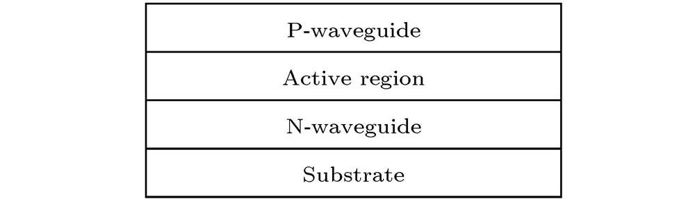
Fig. 1. Epitaxy structure of wafers.外延片结构图
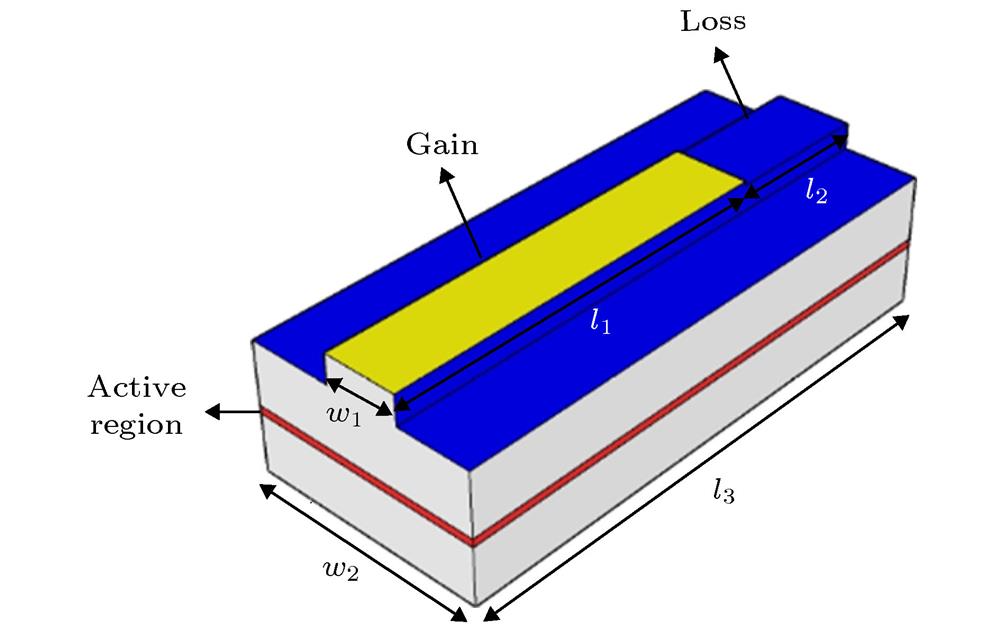
Fig. 2. Device structure diagram, the yellow part is the gain region and the blue part is the loss region.器件结构图, 其中黄色部分为增益区, 蓝色部分为损耗区
Fig. 3. Simulation structure of stripe waveguide.条型波导模拟结构图
Fig. 4. Relationship between wavelength and
when
and
.
折射率虚部为
和
时, 波长与
的关系图
Fig. 5. Relationship between the imaginary part of the characteristic frequency and
when
and
.
折射率虚部为n Ir = –0.01以及n Ir = –0.05时, 特征频率虚部与
的关系图
Fig. 6. Simulation structure of ridged waveguide when length ratio of gain region and loss region is 5∶5, 7∶3, and 8∶2.增益区和损耗区长度比为5∶5, 7∶3以及8∶2时的结构图
Fig. 7. Relationship between wavelength and
when the length ratio is 5∶5, 7∶3, and 8∶2.
长度比为5∶5, 7∶3以及8∶2时, 波长与
的关系图
Fig. 8. Relationship between the imaginary part of the characteristic frequency and
when the length ratio is 5∶5, 7∶3, and 8∶2.
长度比为5∶5, 7∶3以及8∶2时, 特征频率虚部与
的关系图
Fig. 9. Relationship between the normalized intensity and wavelength of cavity modes: (a) The injection current is 100 mA; (b) the injection current is 310 mA (black line), 320 mA (red line) and 330 mA (blue line), respectively.腔模强度与波长关系 (a)注入电流为100 mA; (b)注入电流分别为310 mA(黑线)、320 mA(红线)以及330 mA(蓝线)

Set citation alerts for the article
Please enter your email address
© Copyright 2018-2021 | Chinese Laser Press. All Rights Reserved 沪ICP备15018463号-20