Brian A. Ko, Alexei V. Sokolov, Marlan O. Scully, Zhenrong Zhang, Ho Wai Howard Lee, "Enhanced four-wave mixing process near the excitonic resonances of bulk MoS2," Photonics Res. 7, 251 (2019)
Copy Citation Text
Two-dimensional materials are generating great interest due to their unique electrical and optical properties. In particular, transition metal dichalcogenides such as molybdenum disulfide () are attractive materials due to the existence of a direct band gap in the monolayer limit that can be used to enhance nonlinear optical phenomena, such as Raman spectroscopy. Here, we have investigated four-wave mixing processes in bulk using a multiplex coherent anti-Stokes Raman spectroscopy setup. The observed four-wave mixing signal has a resonance at approximately 680 nm, corresponding to the energy of the A excitonic transition of . This resonance can be attributed to the increased third-order nonlinear susceptibility at wavelengths near the excitonic transition. This phenomenon could open the path to using as a substrate for enhancing four-wave mixing processes such as coherent anti-Stokes Raman spectroscopy.
1. INTRODUCTION
Molybdenum disulfide () is a transition metal dichalcogenide that is generating great interest due to its optical [1–4], electrical [5,6], and catalytic [7,8] properties. Bulk consists of layers of S–Mo–S sheets bonded through van der Waals forces. In bulk form, is a semiconductor with an indirect bandgap of approximately 1.29 eV in the valley. However, in the monolayer limit, the indirect bandgap energy increases and becomes a direct bandgap semiconductor with a bandgap of 1.88 eV at the point [9]. This indirect-to-direct bandgap transition has been studied for its optical effects such as photoluminescence in the monolayer limit [10] and Raman enhancement [11,12].
The advance of monolayer production methods such as micromechanical exfoliation and chemical vapor deposition has led to an increase in the use of thin films to explore various nonlinear optical phenomena [13–15], such as Raman spectroscopy, where charge transfer interactions have been observed to enhance the Raman signal [12]. However, while monolayer has been studied intensively for its ability to enhance nonlinear optical processes, it does have shortcomings. In the Raman enhancement case, the photoluminescence signal of disturbs the Raman signal, resulting in low enhancement of Raman shifts at or near the direct bandgap energy (659 nm) [12]. Monolayer fabrication methods also suffer from low yield, making it difficult to implement commercially. By increasing the layer count and turning into an indirect bandgap semiconductor, the photoluminescence signal becomes quenched while still maintaining the A and B excitonic resonances [10]. Raman spectroscopy measurements capitalizing on the electronic or excitonic resonances of various substrates and samples have been extensively performed, from gases [16] to nanoparticles [17]. In this paper, we present our findings on the observation of the excitonic photoluminescence in bulk via four-wave mixing (FWM). We observe an enhancement of degenerate four-wave mixing near the direct excitonic resonances of using a broadband supercontinuum (SC) coherent anti-Stokes Raman spectroscopy setup (Fig. 1). Previous studies on , especially that of Li et al., have demonstrated nonlinear optical phenomena such as sum frequency generation (SFG) and four-wave mixing [18]. However, our results are performed on bulk substrates, much thicker than the few-layer substrates typically studied. Our results also highlight the enhancement of degenerate four-wave mixing that has not been observed previously. These results show the potential of the excitonic resonances of bulk for enhancement of nonlinear optical phenomena.
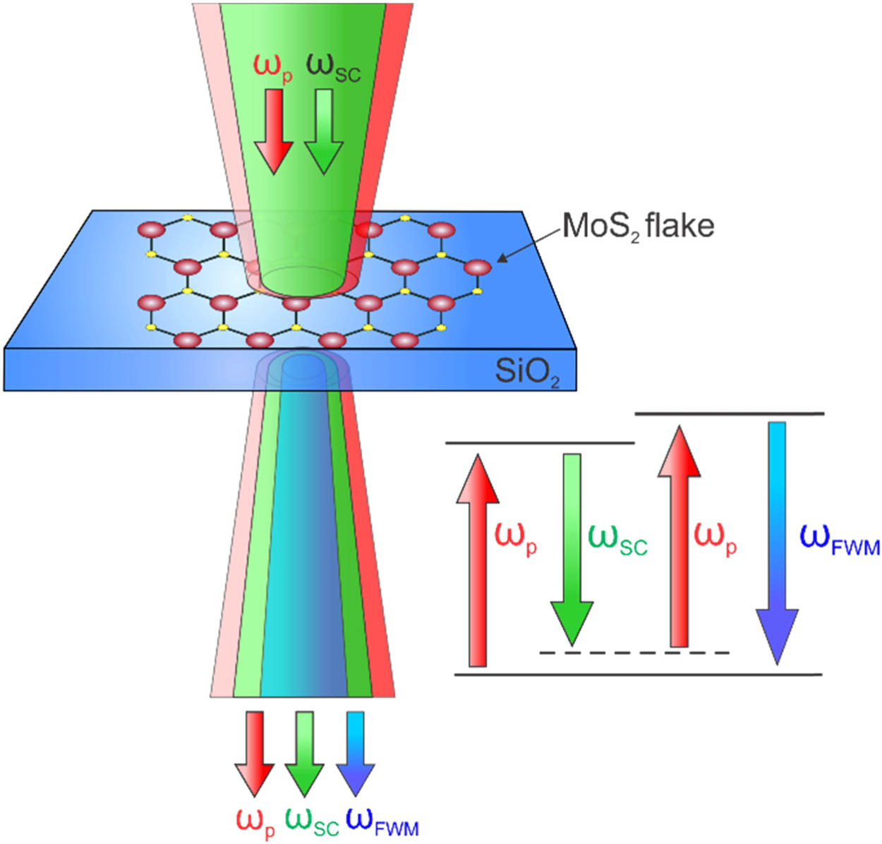
Figure 1.Two pulses ( and ) are incident on an flake. Two photons of the pump pulse () and one photon of the supercontinuum pulse () interact to produce a fourth ().
The flakes were prepared with adhesive tape via mechanical exfoliation and deposited onto a glass slide [19]. Atomic force microscopy (AIST-NT; 40 nm tip diameter) was performed on the flake at the two locations measured to determine flake thickness and layer count (Fig. 2). The measurements determined the minimum thickness of the flake to be 120 nm, with the majority of the flake having a thickness of roughly 290 nm. This corresponds with a layer count between 200 and 600, firmly within the bulk regime.
Sign up for Photonics Research TOC. Get the latest issue of Photonics Research delivered right to you!Sign up now
Figure 2.(a) Atomic force microscope (AFM) image of the flake for the region of interest. (b) Cross section of the flake along the white line in (a).
The optical measurements were performed using a multiplex coherent anti-Stokes Raman spectroscopy setup (CARS-KT, Newport Optics) as shown in Fig. 3. An Nd:YAG laser (Millenia eV) pumps a Ti:sapphire oscillator (Tsunami, Spectra Physics) to produce femtosecond laser pulses (50 fs and 80 MHz repetition rate). The oscillator is mode-locked to produce pulses with a 35 nm bandwidth full width at half-maximum (FWHM) centered at a wavelength of approximately 800 nm. These pulses are split into two pulse trains using a half-wave plate and a polarizing beam splitter. One pulse train is used to pump a photonic crystal fiber to produce a broadband SC pulse with a spectrum ranging from 500 nm to 1100 nm. A long-pass filter is used to filter out wavelengths shorter than 800 nm. The second pulse train is reduced to a 3 nm FWHM pulse centered at 800 nm using a narrow bandpass filter and functions as the pump pulse for the experiment. The two pulse trains recombine at a razor-edge long-pass filter (RELP) and are focused onto the sample. Temporal overlap was achieved using two delay stages to precisely adjust the optical path lengths. Pulse energies for pump and SC pulses before the focusing objective onto the sample were calculated from dividing the measured average power (Thorlabs PM100D power meter with S132C sensor) by the repetition rate of the Tsunami Ti:sapphire oscillator and found to be approximately 6.2 pJ (39 MeV) and 250 pJ (1.56 GeV), respectively. While the SC pulse has over 40 times as much pulse energy as the pump pulse, the bandwidth of the SC pulse is also over 40 times larger than that of the pump. As a result, the pulse energy near a given is comparable to that of the narrowband pump pulse.
Figure 3.Schematic of the multiplex femtosecond coherent anti-Stokes Raman spectroscopy setup. The laser provides 50 fs pulses with an 80 MHz repetition rate. RELP, razor-edge long-pass filter.
The sample was placed on a 3D translation stage, and a camera was used to position the flake normal to the SC pulse in the focal spot. The pump pulse was then manipulated to spatially overlap with the SC pulse. Temporal and spatial overlap of the pump and SC pulses was first confirmed by diverting the two pulses through a beta barium borate (BBO) crystal. Once temporal overlap of the two pulses was achieved, the pulses were then redirected back through the sample for fine temporal overlapping. Temporal overlap was adjusted to maximize the signal at 680 nm and to minimize the effects of the chirp induced by the photonic crystal fiber when generating the SC. The transmitted signal from the sample was filtered using two short-pass filters to remove the excitation wavelengths and free-space coupled into a spectrometer (Horiba iHR 550, 0.78 nm resolution). Spectra at multiple locations on the flake were obtained by moving the flake using the 3D translation stage.
3. RESULTS AND DISCUSSION
Two different locations and thicknesses of the flake are investigated as depicted in the optical microscope image [Fig. 4(a)]. The orange dot corresponds to a thickness of 120 nm, and the blue dot has a thickness of approximately 290 nm. The resultant four-wave mixing spectra at these two locations are shown in Figs. 4(b) and 4(c), respectively. Additional spectra from the flake for different locations are shown in Appendix A. These spectra are characterized by three regions. The green peaks correspond to the Raman mode that appears in bulk [11,20]. The blue region shows a peak at approximately 680 nm with relatively stable peak position as thickness and location on the flake are varied. Lorentzian peak fitting was used to determine individual peak intensities, starting with fitting for the red region. The peak ratio of the 680 nm blue peak to the red peak after Lorentzian fitting is larger for the 290 nm location. The red region shows a large variance in peak position as the excitation location is moved across the flake.
Figure 4.(a) Optical microscope image of the flake. Two different locations with different thicknesses are investigated (blue, 290 nm; orange, 120 nm). FWM signal obtained from the (b) orange spot and (c) blue spot in (a). The FWM spectra are characterized by a large peak (red) with high variance in the center wavelength due to thin film interference, a more stable peak (blue) centered at approximately 680 nm from the excitonic resonances, and a small peak (green) that represents the coherent anti-Stokes Raman signal of .
Single pulse excitation experiments were performed to rule out potential mechanisms for the observed signal. For each region, when the SC pulse train is blocked and only the pump pulse is allowed to reach the sample, the signal obtained is completely quenched (see Appendix B), showing that the process is not the result of two-photon absorption. If two-photon absorption was the driving process for this spectrum, the observed spectra in Figs. 4(b) and 4(c) would be observed if either of the two pulses was incident on the flake [15]. However, when the pump pulse is blocked and the SC is incident on the sample, a resulting spectrum similar to the ones shown in Fig. 4 is obtained but with lower intensity. We attribute this to leakage of the SC pulse through the short-pass filters after the sample.
To determine the effects of individual pulses on the observed spectrum, a variable neutral density filter was placed in the path of either pulse train to control the pulse energy without modifying the spectral character of the pulse. Average power was recorded, and delay stages were modified between measurements to adjust peak temporal overlap as the pulse energy was changed (Fig. 5). As incident power is changed, there is no noticeable shift in the spectral character of the resultant signal (insets). The measurements were performed at the location with a 290-nm-thick spot since it provides a more well-defined peak at 680 nm than the thinner section. Spectra obtained using variable input powers were analyzed by Lorentzian fitting to obtain the peak area of the 680 nm peak and plotted with respect to average incident power of the pulses as shown in Figs. 5(a) and 5(b) (red dots). The results were then fitted via a polynomial fitting, and the intensity dependence due to the relation between the intensity of an observed spectrum and the intensities of the incident pulses was described as where and are the number of photons from the pump and SC pulses required to produce the observed signal, respectively. As seen in Fig. 5(b), the observed signal had a linear dependence on the SC intensity, indicating that one SC photon is required. In contrast, a quadratic dependence on the incident intensity of the narrowband pump pulse is observed [Fig. 5(a)], indicating that two pump photons are required in the emission process. A linear component was also observed, possibly due to a low amount of transmission through the short-pass filters after the flake. This process was repeated for the 120-nm-thick location, and the results were consistent with that of the 290-nm-thick location. This indicates that the observed spectrum results from a third-order, four-wave mixing process.
Figure 5.Photoluminescence intensity dependence for (a) pump and (b) supercontinuum pulses on the 290 nm section of the flake. The quadratic dependence of the FWM signal on the pump power corresponds to requiring two pump photons for the process, while the linear dependence on the supercontinuum indicates that a single supercontinuum photon is used. Insets show the photoluminescence spectrum as pulse power is modulated. Enlarged insets can be found in Appendix C.
With the required number of photons from each pulse train known, the four-wave mixing relation for the observed signal was obtained by modifying the SC spectrum into a narrowband pulse and varying its wavelength range using different bandpass filters (850 nm, 900 nm, 950 nm, 1000 nm; 10 nm FWHM). These bandpass filters were placed in the path of the SC before the razor-edge long-pass filter, and temporal overlap was readjusted with each filter for peak signal intensity (Fig. 3). The resultant four-wave mixing signal changes to a narrow peak in the presence of a bandpass filter because the range of the SC pulse is restricted to a narrow band. The resultant spectra are shown in Fig. 6. With the 850 nm bandpass filter, the resultant FWM peak is located at 768 nm, while with the 900 nm filter, the FWM peak is found at 730 nm. These measurements confirm that the four-wave mixing relation for the observed signal is The pump wavelength was determined to be approximately 807 nm during these measurements. This four-wave mixing relation has multiple analogous excited state diagrams. To distinguish between these processes, we would need to determine through which electronic state coherent propagation of the observed process is occurring, using for example a three-pulse four-wave mixing process. A third pulse train obtained by splitting the pump pulse into two pulses with a beam splitter, along with an additional delay line, is necessary [21]. Our experimental setup is not capable of discerning this due to the lack of the third pulse train. Interestingly, this is the same four-wave mixing frequency relation as that of coherent anti-Stokes Raman scattering. However, the observed spectra outside the green CARS region in Fig. 4, especially the 680 nm peak in the blue region of Fig. 4, do not correspond to the excitation of a known Raman mode of [11]. Therefore, the resultant spectra occur due to a property of not related to its vibrational modes.
Figure 6.Four-wave mixing spectra of the flake with different bandpass filters placed in the supercontinuum pulse path. The numbers indicate the central wavelength of the filters, and the pump pulse is located at wavelength of 806 nm.
Because of the observed four-wave mixing relation, one possible cause for the variation of the red peak in Fig. 4 is shifts in the SC intensity at wavelengths that would produce the observed peaks. The SC spectra at the two locations shown in Fig. 4(a) were measured by removing the short-pass filters used to remove the two incident pulses after the sample and directly measuring the SC pulse spectrum (see Appendix D). A neutral density filter was placed near the spectrometer in order to prevent signal saturation of the spectrometer without affecting the overall character of the observed SC spectrum. The SC spectrum while on the 120-nm-thick portion of the flake is characterized by a broad background signal with peaks at 855 nm, 870 nm, 882 nm, 900 nm, and 942 nm. When moving to the 290-nm-thick portion, the background for the SC pulse changes, but the positions of the peaks of the SC remain relatively unchanged. Moreover, the relative intensity ratios of these peaks varied depending on the thickness of the flake. This confirms that thin film interference effects occur within the flake. These thin film interference effects occur because , where is the refractive index of , is the thickness of the flake, and is the wavelength of the incident light. The layered structure of the flake, which can be viewed as multiple flakes of intermediate thicknesses stacked together, causes varying interference rates for different wavelengths of the SC pulse [22]. The interference effects are affected by the layer–layer spacing of the flake at that position, as well as the angle of incidence of the laser pulses, such that small translations across the flake can change the interference rate. As a result, the spectrum of the SC pulse changes with its location on the flake. These modified SC pulses then interact with the 800 nm pump pulse to produce different nonresonant four-wave mixing signals as the location is changed. However, the relatively stable peak position of the 680 nm peak in Figs. 4(b) and 4(c) implies that this peak is unaffected by thin film interference effects. This leads to the conclusion that this peak is determined by the intrinsic properties of , such as the direct excitonic transitions within the semiconductor.
From previous works on the band structure of [1–4,9,23], has direct excitonic resonances of 1.88 eV and 2.04 eV at the point, called the A and excitons, respectively. In the monolayer limit, the A exciton becomes the lowest energy transition between bands, and becomes a direct bandgap semiconductor. As layer count increases, becomes an indirect bandgap semiconductor with a bandgap between 1.3 eV and 1.6 eV [9]. However, the direct excitonic resonances are mostly unchanged in energy in the bulk limit because the direct resonances are dependent on the localized d orbitals of the atoms, making them less sensitive to layer thickness [24]. Near these resonances, light-induced transitions between the conduction and valence bands generate a large concentration of free carriers that exhibit the spatial variations of the incident electric field, resulting in perturbations of the refractive index that can lead to an increase of several orders of magnitude of the third-order susceptibility [25]. This increased value leads to an increased intensity of the measured four-wave mixing signal, resulting in the peak observed in the blue-colored region near 680 nm (1.88 eV, A exciton) in Fig. 4. Similarly, we also observe a second, but much weaker, peak centered at approximately 595 nm, corresponding to the B exciton of (2.04 eV) (see Appendix E). This signal is weaker due to the higher energy requirement of the B exciton and the lower SC intensity at the wavelength required for the four-wave mixing process at 2.04 eV. Likewise, higher energy excitons, such as the C and D excitons that arise through transitions between the deep-valence bands and the conduction band [26], do not play a large role as the four-wave mixing condition requires a Stokes wavelength well outside the range of our SC pulse. These resonances can be used to enhance four-wave mixing processes on the surface of the flake by creating large electric fields at wavelengths near the bandgap to induce localized surface plasmons [27].
Wang et al. observed that the intensity of the third-harmonic generation (THG) signals from displayed a quadratic dependence on flake thickness and that the THG was quenched in the monolayer limit [24]. Similarly, we also observe the four-wave mixing photoluminescence peak to be quenched when measuring a commercial solution of nanoparticles with thicknesses generally at or near a monolayer. The relative intensity of the 680 nm FWM peak was also observed to be higher for the 290 nm portion of the flake, even with the decreased transparency of the higher thickness. Calculation of the third-order nonlinear susceptibility (see Appendix G) yields a result on the order of , which is in agreement with previous experimental works by Wang et al.[24] and Woodward et al.[28] as well as Soh et al.’s theoretical work [29]. Our results on enhanced photoluminescence via excitonic resonances of could open the path for enhancing four-wave mixing processes of for optical sensing and imaging applications such as coherent anti-Stokes Raman spectroscopy.
4. CONCLUSION
A photoluminescence-like signal from bulk was observed via four-wave mixing. Pulse power dependence measurements confirmed the four-wave mixing relation between the broadband SC and the 800 nm pump pulse. The signal arises due to the increased third-order nonlinear susceptibility near excitonic resonances in semiconductors as light–matter interactions cause perturbations in the refractive index at wavelengths near these resonances. From these measurements, a third-order nonlinear susceptibility on the order of is calculated, in agreement with other measurements performed previously. This opens the path to using bulk for nonlinear optical processes as increasing the layer count quenches the photoluminescence peak while still retaining the excitonic resonances that create the photoluminescence. This provides a strong case for resonant Raman enhancement using bulk .
Acknowledgment
Acknowledgment. Z. Z. and H. W. H. L. designed and conceived the project. B. K. performed measurements. M. O. S., Z. Z., and H. W. H. L. supervised the project. All authors wrote the paper, discussed the results, and commented on the manuscript.
The authors declare no competing financial interests.
APPENDIX A: FOUR-WAVE MIXING SPECTRA OBTAINED FROM
Spectra were obtained by moving the flake using the 3D translation stage in order to measure the signal from multiple locations. Figures 7(b) and 7(c) show the four-wave mixing spectra of different locations marked in Fig. 7(a).
Figure 7.(a) Optical microscope image of the flake. (b) Four-wave mixing spectra obtained at positions A–C marked in (a). (c) Four-wave mixing spectra obtained at positions D–F marked in (a).
Figure 8.Spectrum obtained at the two locations depicted in Fig. 4(a) by blocking individual pulses. Unblocked spectrum (both pulse trains) is shown in black, supercontinuum only (pump blocked) in blue, and pump only (supercontinuum blocked) in red.
Figure 9.Spectra (solid lines) and fitted peaks (dashed lines) of the flake as the power of each pulse is modulated (other pulse’s power held constant). Lorentzian peak fitting was done on each spectrum and the area of the 680 nm peak was calculated.
Figure 10.Measured spectrum of the supercontinuum pulse incident on the (a) blue and (b) orange spots in Fig. 4(a). Spectra were obtained by blocking the pump pulse and removing the short-pass filters that block the incident pulses. A neutral density filter was placed to prevent saturation while maintaining the spectral character.
Figure 11.B excitonic resonance of at the blue spot of Fig. 4(a) (thickness of 290 nm). The energy of the B exciton corresponds to a wavelength of approximately 600 nm.
APPENDIX B: MEASURED SPECTRA OF THE MoS2 FLAKE WIT
One of the two incident pulse trains was blocked to determine the mechanism behind the resultant spectra (Fig. 8). When the SC pulse is blocked and only the pump remains (red spectra), no four-wave mixing occurs, confirming that the observed process is not the result of two-photon absorption. Similarly, when only the SC is allowed to excite the flake, we observe a signal but, overall, no four-wave mixing. We attribute that to some of the SC pulses transmitting through the short-pass filters after the sample.
APPENDIX C: MEASURED SPECTRA OF THE MoS2 FLAKE WIT
The power of one of the two incident pulse trains was modulated using a variable neutral-density filter (Fig. 9). Temporal overlap was adjusted for maximum signal intensity. Lorentzian peak fitting was performed to isolate peak areas, which were then plotted to determine the dependence of the resultant four-wave mixing signal on the individual pulses (Fig. 5).
APPENDIX D: SUPERCONTINUUM SPECTRA AT DIFFERENT LO
To confirm that the red peaks in Figs. 4(b) and 4(c) are the result of thin film interference effects on the SC pulse, the pump pulse was blocked and the short-pass filters after the sample (see Fig. 3) were removed. A neutral density filter was placed before the spectrometer to prevent saturation while preserving the overall spectrum. As the flake position was changed, the intensity of the SC at different wavelengths changed at different rates, producing different SC spectra (Fig. 10). The SC then interacts with the pump pulse to produce nonresonant four-wave mixing peaks of varying peak location.
APPENDIX E: B EXCITONIC RESONANCE
The B excitonic resonance of is also observed (Fig. 11). The B exciton of has an energy of 2.06 eV, corresponding to a wavelength of 600.1 nm. We observe a much smaller peak at 600 nm when the pulses are incident on the blue spot of Fig. 4(a). The smaller intensity of the B exciton can be attributed to the decreased probability of a transition of higher energy than the A exciton (1.88 eV) and the lower intensity of the SC pulse at the wavelengths required to produce four-wave mixing near the B exciton (approximately 1200 nm).
APPENDIX F: THICKNESS DEPENDENCE OF THE FOUR-WAVE
Starting with the coupled-wave equations for degenerate four-wave mixing with the undepleted pump and slowly varying envelope approximations, the wave equations become [30] where where is the vacuum impedance and the third-order nonlinear susceptibility in a semiconductor at photon energies near the bandgap for a short laser pulse is [25] where is the effective electron-hole mass, is the absorption coefficient of , is the quantum efficiency of carrier generation, and is the local carrier lifetime.
Solving the coupled-wave equations yields Therefore, ~where is the thickness of the material. Because the intensity I is proportional to , we predict a quadratic dependence on the thickness of the flake.
APPENDIX G: CALCULATION OF THE THIRD-ORDER NONLINE
The third-order nonlinear susceptibility in a semiconductor at photon energies near the bandgap for a short laser pulse (pulse duration ) is [25] where is the effective electron-hole mass, is the refractive index, is the absorption coefficient of , is the quantum efficiency of carrier generation (of order unity), and is the incident pulse duration.
For the A excitonic resonance of at 680 nm, is 0.24245me [31], is 5.878 [32], is , and is . Substituting into the above equation yields the upper bound for , assuming a quantum efficiency of 1: Using the absolute intensity of the 680 nm peak observed in the 290 nm area, we can derive the average power generated by the four-wave mixing process:~Substituting the absolute intensity for the 680 nm peak and accounting for absorption by the flake, we get an average power of .
The average power of a laser pulse can be related to its irradiance via where is the repetition rate, is the pulse duration, and is the spot size. Likewise, the irradiance can be expressed via the field amplitude : Combining the two equations yields where for 80 MHz repetition rate, 35 fs pulse duration, and 7.5 μm spot size.
Also, for a four-wave mixing process, the FWM field amplitude is related to the incident field amplitudes via Thus, Substituting experimental conditions and indexes of refraction for the three wavelengths [32] results in which is in general agreement for the bulk nonlinear susceptibility at the A exciton resonance found by other methods [28,33].
Brian A. Ko, Alexei V. Sokolov, Marlan O. Scully, Zhenrong Zhang, Ho Wai Howard Lee, "Enhanced four-wave mixing process near the excitonic resonances of bulk MoS2," Photonics Res. 7, 251 (2019)