1Guangdong Provincial Key Laboratory of Optical Fiber Sensing and Communications, Institute of Photonics Technology, Jinan University, Guangzhou 510632, China
2College of Electronic Science and Technology, Shenzhen University, Shenzhen 518060, China
We show that a metasurface composed of a subwavelength metallic slit array embedded in an asymmetric dielectric environment can exhibit either extraordinary optical transmission (EOT) or extraordinary optical diffraction (EOD). The cascaded refractive indices of the dielectrics can leverage multiple decaying passages into variant subsections with different diffraction order combinations according to the diffraction order chart in the k-vector space, providing a flexible mean to tailor resonance decaying pathways of the metallic slit cavity mode by changing the wavevector of the incident light. As a result, either the zeroth transmission or st reflection efficiencies can be enhanced to near unity by the excitation of the localized slit cavity mode, leading to either EOT or EOD in a single structure, depending on the illumination angle. Based on this appealing feature, a multifunctional metasurface that can switch its functionality between transmission filter, mirror, and off-axis lens is demonstrated. Our findings provide a convenient way to construct multifunctional miniaturized optical components on a single planar device.
Integrating various functionalities on a single miniaturized photonic device can largely simplify the overall optical system design, and therefore is a continuing trend in the nanophotonic area. There are many ways to realize multifunctional devices, such as the so-called “Janus” transformation optics device [1], acting as either a lens or a beam-shifter; parity-time-symmetric multilayers, which can simultaneously support extraordinary transmission and reflection [2]; and a single parity-time-symmetric cavity that can support both lasing and anti-lasing [3]. Those demonstrations require large coherent interaction lengths during light’s propagation in such devices.
Recently, exploring various wavefront-shaping functionalities in a single ultrathin layer, i.e., metasurface, has been widely studied in the nanophotonic field due to the easy fabrication of a flat monolayer instead of a three-dimensional bulky structure [4–6]. Resorting to the abrupt phase change of each resonant element instead of accumulated interaction with large coherent length between light and structure, the ultrathin metasurface can provide various applications, such as beam deflection [7–11], focusing [12–16], complex beam shaping [17–23], holographic display [24–29], and multiplexed hologram recording [30–39]. In particular, single metasurfaces with multiple functionalities represent a newly emerging research frontier and receive onrushing developments [40,41]. Generally, the previous metasurface with high efficiencies can only work on either transmission mode [7] or reflection mode [9,27] depending on the limited number of deterministic decaying pathways. For transmission metasurfaces [42,43], only the transmission decaying channel is used for wavefront manipulation, while the reflection decaying channel is abandoned. For reflection metasurfaces [44,45], a metallic mirror is usually placed below the metasurface nanostructure to block all transmission channels, and only the reflection channel is tailored on demand. A metasurface with versatile functionalities demands multiple decaying pathways of its resonance, which inevitably leads to the tradeoff between functionalities and efficiencies owing to the competition among different decaying passages. In this paper, we present a metallic slit metasurface that harnesses both the transmission and reflection decaying channels of different diffraction orders, and demonstrate angularly switchable functionalities with nearly unitary efficiencies.
It is well known that, for a metallic slit array with subwavelength period (), the localized resonance mode in the slit area leads to the enhanced transmission of incident light, which is known as extraordinary optical transmission (EOT) [46,47]. To obtain unitary diffraction efficiency of a grating, the usual method is to mimic a blazed grating by making a gradient phase profile with a discrete set of different nanoresonators in a large supercell [7,48,49]. Very recently, it has been shown that metasurfaces with identical unit cells, rather than the gradient phase approach, are also capable to obtain near-unitary diffraction efficiencies by harnessing the decaying pathways of the resonance cavity mode into high diffraction orders [20,50,51], which is referred to as extraordinary optical diffraction (EOD) [20]. Now, we consider a metallic subwavelength slit array embedded in an asymmetric dielectric environment exhibiting cascaded refractive indices without a metallic ground plate, and demonstrate that both EOT and EOD can happen in a single structure. According to the diffraction order chart in k-vector space, the resonance decaying pathways of the slit cavity mode can be tuned to either zeroth transmission or st reflection channel by changing the parallel wavevector of incident light. As a result, the metasurface exhibits resonantly enhanced transmission for small incident angles, acting as a transmission filter; exhibits total internal reflection (TIR) for moderate incident angles, acting as a refection mirror; and exhibits EOD for large incident angles, which can be applied for arbitrary wavefront shaping, such as deflecting, focusing, beam shaping, and hologram displaying. Such metasurfaces with versatile functionalities harnessing of multiple decaying channels are fundamentally different from the previous work based on single diffraction order enhancement approaches [20,40,50,52]. The demonstrated capability to control both the transmission and reflection channels of impinging light of our proposed metasurface provides a convenient and efficient way to realize multifunctional miniaturized optical components on a single surface.
Sign up for Photonics Research TOC. Get the latest issue of Photonics Research delivered right to you!Sign up now
2. MODE EXPANSION THEORY MODEL
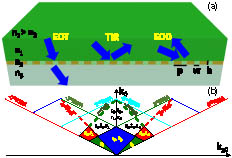
Figure 1(a) illustrates the schematic of the multifunctional metasurface, which is a metallic subwavelength slit array (with slit width , slit height , and period ) embedded in an asymmetric environment. The refractive index of the medium in the incident side is larger than that of the medium in the transmission side () to make sure that there are intersection areas that are not only higher than zeroth reflection Woods anomaly (RWA) but also lower than zeroth transmission Woods anomaly (TWA) [green and red patches in Fig. 1(b)]. The refractive index in the slit area is chosen properly so that the resonance wavelength of the slit cavity mode can cross all three kinds of areas with truncated diffraction order combinations, which are marked as blue, green, and red patches in Fig. 1(b). For small, moderate, and large incident angles, the beam will undergo EOT, TIR, and EOD, respectively, as the decaying pathways of the slit cavity mode are composed by different diffraction order combinations for different angles. Assume a plane wave with wavenumber and parallel wavevector illuminating the structure from the superstrate; the possible propagating diffraction orders for both reflection () and transmission () can be found in the diffraction order chart as shown in Fig. 1(b). The diffraction order chart is constructed by RWA (solid) and TWA (dashed) lines, which are governed by the equations and ( is an integer), respectively. Above the th () RWA/TWA, the propagating reflection/transmission of the th diffraction order () begins to appear, while below the zeroth RWA, which is also known as the light line, there are only evanescent waves without any radiation. For simplicity, we only consider the lowest areas of the diffraction order chart, where only a few diffraction orders (0 and ) exist. In the lowest sidelobe areas (green patches), there is only a channel, where TIR happens; in the lowest central area (blue patch), there are only two propagating channels of and , which may give rise to EOT; and in the higher sidelobe areas (red patches), there are only two propagating channels of and , allowing for the possibility of EOD. As the diffraction order chart is symmetric with respect to the axis, we only consider the case in the following discussions.
Figure 1.(a) Schematic of the metasurface structure that can exhibit EOT, TIR, or EOD, depending on the incident angle. The index of the upper layer, slit area, and lower layer is , , and , respectively. (b) Diffraction order chart in k-vector space of the structure in (a). Solid lines represent the RWAs with orders , , and , while the dashed lines represent TWAs with orders , .
To obtain the transmission and reflection spectra of different diffraction orders, we first employ the analytical model expansion theory by considering the metal as a perfect electric conductor (PEC) [20,53]. When a plane wave with parallel wavevector and transverse magnetic (TM) polarization illuminates on the metallic slit array, by matching the boundary conditions, which require that the tangential components of both the electric field () and the magnetic field () are continuous at interfaces, we can analytically obtain the zeroth reflectance , zeroth transmittance , and st reflectance with closed forms as follows (see Appendix A): where, , , and are the permittivities of the upper layer, slit area, and lower layer, respectively; and are forward and backward complex amplitude coefficients of the cavity mode in the subwavelength slit area, which can be obtained by solving linear equations with where , is the wavevector of the incident plane wave, and , () is the wavevector of the th diffraction order in the superstrate and substrate, respectively.
3. RESULTS AND DISCUSSION
Figures 2(a)–2(c) show the analytically obtained , , and for varying wavelengths and incident angles, by Eqs. 1(a)–1(c), respectively. The parameters of the metallic slit array are chosen as μ, μ, μ; the refractive indices of the upper layer, the slit area, and the lower layer are , , and , which can be realized by silicon nitride, silica, and air, respectively. In Fig. 2(a), there are three abrupt color changing contours, which correspond to the zeroth TWA (critical angle for TIR), st RWA, and st TWA in Fig. 1(b), respectively. The subareas ① (upper-left), ② (upper-middle), and ③ (upper-right) in Fig. 2(a) separated by those WA lines correspond to the blue patch, green patch, and red patch in Fig. 1(b), respectively. Thus, there are only and channels in ①, only in ②, and only , channels in ③, respectively. We see that exhibits dips in subareas ① and ③, at the resonant wavelength of about 3.3 μm, which corresponds to the fundamental cavity mode in the metallic silts. For different incident angles, the resonant wavelength stays the same, because the slit cavity mode that leads to the resonant dip of is a localized resonant mode, whose excitation is independent of the incident angles. Correspondingly, exhibits a resonant peak approaching unity at the same position of the dip in subarea ① [] as shown in Fig. 2(b). Note that the subarea ① is the widely studied zeroth-order-diffraction zone in the metamaterial community; many phenomena such as EOT [46], the generalized Brewster effect [54–56], and perfect absorption [57] are found in this zone, while the influence of the resonance behavior on areas other than subarea ① receives scarce attention. When , is always zero because the incident angle is larger than the critical angle for TIR. Figure 2(c) shows that also exhibits a peak at the same position of the dips in subarea ③. Therefore, the slit cavity mode indeed can enhance the diffraction efficiency of the st order to near unity, as long as the propagating channels are restricted to only and . We note that, between the EOT and EOD, there is a transitional area (subarea ②), where is constantly unity [Fig. 2(a)]. This is due to the fact that is the only propagating channel in this subarea; the resonant behavior of the slit cavity can only lead to a phase change of the reflection coefficient, while the reflection amplitude always stays unity. However, when the absorption loss channel is considered in the practical case, there may be a resonant absorption phenomenon that can also lead to the dip in subarea ②.
Figure 2.Analytical results of (a) zeroth reflectance , (b) zeroth transmittance , and (c) st reflectance , respectively, of the metasurface for varying incident angle and wavelength . The three abrupt color changing contours in (a) automatically show the critical angles for TIR, the st RWA, and the st TWA, respectively, as marked in the figure, and they split the whole phase map into different subareas that contain combinations of different propagating channels (also denoted in the figure). In subarea ①, there are and channels; exhibits a dip in (a), while exhibits a peak in (b) under the resonance condition of the slit cavity mode. In subarea ②, there is only a channel; is unity in the whole subarea. In subarea ③, there are and channels; exhibits a dip in (a), while exhibits a peak in (c) under the resonance condition of the slit cavity mode.
According to the theory we discussed above, now let us consider the practical case of real metallic structures. Silver is chosen as the metal material due to its small ohmic losses. The permittivity of silver is obtained by fitting the experimental data [58] to the Drude model. Figure 3 shows the , , and spectra by the finite element method (FEM), which is implemented by the commercial package COMSOL. At incident angles of 0° [Fig. 3(a)] and 15° [Fig. 3(b)] that belong to the subarea ①, (green) exhibits resonant dips below 0.1, while (blue) exhibits peaks exceeding 0.9 at the wavelength of about 3.3 μm, which is the typical EOT phenomenon. At the incident angle of 35° [Fig. 3(c)] that belongs to the subarea ②, both and are suppressed as zero, while is the only nonzero value after the Wood’s anomaly wavelength (μ). At incident angles of 45° [Fig. 3(d)] and 60° [Fig. 3(e)] that belong to the subarea ③, (green) also exhibits resonant dips at the wavelength around 3.2 μm, while (red) exhibits resonant peaks exceeding 0.9 at the corresponding wavelength, which is the EOD phenomenon. We note that there are sharp peaks for and sharp dips for with Fano lineshape at the short wavelength side in Figs. 3(b)–3(d), which is due to the Wood’s anomalies near those wavelengths. Compared with the model expansion theory results [dashed lines in Fig. 3], the peak values of and of the FEM simulation results are slightly lower, and the resonant wavelength shifts a little to shorter wavelengths, because the real metal inevitably has absorption loss and finite negative permittivity, which give rise to overall power loss and the decrease of the effective wavelength of the slit mode. Nevertheless, the FEM simulation results for real metal (solid lines in Fig. 3) are generally consistent with the theoretical results (dashed lines in Fig. 3). The appearance of the EOT and EOD relies on the different resonant decaying pathways (zeroth or st diffraction order channels) of the local slit cavity mode; therefore we can tailor the working wavelength and bandwidth of EOT and EOD through the slit parameters in the wavelength range , where all three kinds of subareas ①, ②, and ③ can be reached.
Figure 3.Reflection () and transmission () spectra of the metasurface composed of real metal (silver), for different incident angles (a) , (b) , (c) , (d) , and (e) , respectively. Dashed curves show the corresponding analytical results of the PEC metasurface for comparison.
In general, the resonant wavelength is linearly dependent on the slit height , and the bandwidth is positively correlated to the slit width . Thus, the proposed structure can tailor the working condition of the multiple functionalities on demand.
To clearly illustrate the evolution from EOT to EOD, we fix the working wavelength at 3.3 μm, and plot the , , and as a function of the incident angle as shown in Fig. 4(a). In the practical experimental setup, the apparatus to steer the beam angle can be facilely realized by many methods, such as scanning mirror, rotational stage under the metasurface, or circular rail under the illumination source [38,59]. It indicates that, as we gradually increase the incident angle from 0° to 90°, the beam first undergoes EOT (; ). And after the critical angle of 30°, the beam experiences TIR, where is the only nonzero component. To further increase the incident angle to cross the st RWA line (), the EOD begins to happen, where becomes the largest component, while and are effectively suppressed. Figures 4(b)–4(f) show the field patterns () for a Gaussian beam illuminating the metasurface with different incident angles, which are calculated by the COMSOL package. We can clearly see that, for small incident angles (0°, 15°), the beam passes through the metallic slit metasurface [Figs. 4(b) and 4(c)] even if the slit width is in deep subwavelength range (μμ), and the relation between the transmission angle and incidence angle obeys the Snell law (). For incident angle 35° in subarea ②, the incident beam undergoes ordinary TIR, with the reflection angle equal to the incident angle [Fig. 4(d)]. For large incident angles (45°, 55.6°) in subarea ③, the incident beam undergoes negative reflection, with the reflected beam on the same side of the incident beam with respect to the normal [Figs. 4(e) and 4(f)], which is the typical behavior of EOD. Retroreflection occurs when the incident angle is 55.6° (Littrow mount angle); that is, the beam is reflected back along its original path, even for oblique incidence [60]. Note that the beam width of the incident beam is set as , which gives the divergence angle of 5°; the above simulation results reveal that such a small divergence angle has little influence on the angular tailoring of multiple functionalities. In a realistic experiment, the footprint of the proposed metasurface can be designed on the order of 200 μm by 200 μm, which can be compatible with a weakly focused Gaussian beam with a small divergence angle limited to less than 5° (for example, beam width 10 mm together with a lens focal length gives a divergence angle of about 2°).
Figure 4.(a) Reflection (, ) and transmission () as a function of the incident angle at the working wavelength μ for the periodic slit array of which the zoom-in structure is shown in the upper panel. Dashed curves show the corresponding analytical results of PEC metasurface for comparison. (b)–(f) Field patterns () of a Gaussian beam with μ illuminating the metasurface (the area marked by the red dashed frame) with different incident angles: (b) 0°, (c) 15°, (d) 35°, (e) 45°, and (f) 55.6°, respectively.
Based on EOD, we can design arbitrary wavefront-shaping metasurfaces with the binary computer-generated hologram approach [61]. As an example, we design a multifunctional metasurface that can behave as an off-axis lens in the EOD domain by modulating the metallic slit array with a quadratic phase profile . The modulated structure is based on the periodic grating structure with geometric parameters μ, μ, and μ; after the modulation, both the slit width and the period of the grating will exhibit linear gradient profiles as shown in Fig. 5(a). For small incident angles [Figs. 5(b) and 5(c)], the beam still can pass through the nonperiodic subwavelength slit array, exhibiting the EOT phenomenon. For the incident angle of 35° [Fig. 5(d)], the metasurface acts as an ordinary mirror, making the incident beam undergo TIR. For large incident angles [Figs. 5(e) and 5(f)], the metasurface becomes an off-axis lens, which can focus the incident beam into a single line in the st diffraction direction, while the specular reflection in the right side is near-totally suppressed. Therefore, for different incident angles, the metasurface indeed can act as an optical device with totally different functionalities. This angle-dependent multifunctional device may be potentially useful in panoramic viewing systems. Although we only designed 1D functional devices, arbitrary 2D wavefront-shaping devices can also be obtained by modulating the structure in both and directions according to a predefined phase profile, which typically results in a curved grating profile [20].
Figure 5.(a) Schematic of the modulated metasurface with a gradient grating profile with a zoomed-in structure on the upper panel. (b)–(f) Field patterns () of a Gaussian beam with μ illuminating the modulated metasurface (the area marked by the red dashed frame) with different incident angles: (b) 0°, (c) 15°, (d) 35°, (e) 45°, and (f) 55.6°, respectively. In (b) and (c), the incident beam also undergoes EOT. In (d), the incident beam still undergoes TIR. In (e) and (f), the incident beam undergoes the focusing capability, with near-total suppression of the zeroth diffraction order.
In conclusion, we show that a metallic subwavelength slit array embedded in an asymmetric environment can support EOT, TIR, and EOD simultaneously. The cascaded dielectric environment can leverage multiple decaying passages into variant subsections with truncated diffraction order combinations according to the diffraction order chart in the k-vector space, which allows the wavevector-dependent tunneling of the slit cavity mode to different diffraction orders. For small incident angles, the resonance decaying pathway goes to the zeroth transmission channel, giving rise to enhanced transmission to near unity, while for large incident angles, the resonance decaying pathway switches to the st reflection channel, leading to enhanced diffraction to near unity. Between the EOT and EOD areas, there is also a transitional area with moderate incident angles, where ordinary specular reflection happens. Based on the above theory, a multifunctional metasurface that can behave as a transmission filter, a mirror, and an off-axis lens simultaneously is demonstrated. Our proposed metasurface can be used to realize multifunctional optical components on a single planar device.
APPENDIX A
To deduce Eqs. (1)–(3) in the main text, let us consider that a plane wave with an arbitrary incident angle (or parallel wavevector ), where TM polarization (magnetic field is always parallel to the slit direction) illuminates the structure from the superstrate. Owing to the diffraction effect of the grating, the electromagnetic (EM) field in the superstrate and the substrate can be expanded as plane waves of all diffraction orders (including both propagating and evanescent components). As a result, the transverse EM field components in the superstrate and the substrate have the following forms: where , is the wavevector of the incident plane wave, and , () is the wavevector of the th diffraction order in the superstrate and the substrate, respectively. and are the complex transmission and reflection coefficients for the th diffraction order, respectively. is the permittivity of vacuum; is the angular frequency, and is the amplitude of the incident wave.
In the slit area, there are generally multiple waveguide modes in each metallic slit. However, for the ultra-narrow slit in the deep subwavelength scale, the higher order modes are cut off, and hence only the fundamental mode needs to be considered. We assume and are the forward and backward amplitude coefficients in each slit, respectively; then the transverse EM field components in the metallic slit area are where is the rectangular function, and the amplitude coefficients and are unknown variables that can be determined by the boundary condition requiring that the parallel EM field components should be continuous at all interfaces.
At the interface , the boundary condition yields and at the interface , the boundary condition yields
Considering the orthogonality of different diffraction orders, we multiply Eqs. (A4b) and (A5b) by and then integrate over , respectively. This yields
Thus, , can be expressed in terms of , as
Multiplying Eqs. (A4a) and (A5a) by and then integrating in terms of in region , respectively, yields
Substituting Eqs. (A7a) and (A7b) into Eqs. (A8a) and (A8b), respectively, yields
From Eq. (A9), we can build a matrix with elements as expressed in Eq. (3) in the main text.
Then, the amplitude coefficients of cavity modes in metallic slits can be solved by a linear matrix equation, , where . Finally, substituting the solved amplitude coefficients and back into Eq. (A7), we can readily obtain the reflection and transmission coefficients for arbitrary diffraction orders.
In the main text, we focus on the zeroth reflection , zeroth transmission , and st reflection . They can be analytically expressed as
The corresponding power reflectance and transmittance are , , and , respectively, which are exactly the expressions in Eq. (1) in the main text.