Junqiang Shao, Xueting Yuan, Zelin Mu, Gang Ni. Magnetic field effects in organic light-emitting diodes with Co electrode[J]. Chinese Optics Letters, 2016, 14(6): 062501
Copy Citation Text
Tris-(8-hydroxyquinoline)-aluminum –based organic light-emitting diodes with Co electrode are fabricated. The positive magnetic electroluminescence (MEL) and magnetic conductance (MC) are observed in the samples, reaching 4.35% and 1.67% under the field of 42 mT at 50 K, respectively, and the MEL and MC traces can be fitted to non-Lorentzian line shapes. The MEL varies as a function of the Co thickness and reaches the optimal value at 10 nm. The MEL and MC dependence on voltage and temperature is also investigated. The electron-hole pair model and the spin-polarized injection mechanism are used to understand the experimental results.
During the past decade, the influence of magnetic fields on the transport properties and electroluminescence (EL) of organic light-emitting diodes (OLEDs) has attracted much attention[1]. Many models have been proposed to understand the magnetic field effects (MFEs) in OLEDs, such as the electron-hole pair model, the bipolaron model, and the triplet-polaron interaction model. However, the underlying mechanisms of the MFEs are still under debate. Even though various experimental and theoretical studies have been carried out extensively on the conventional, nonmagnetic OLEDs, there are only a few reports on OLEDs with magnetic electrodes in the beginning[2–4]. As we know, EL in OLEDs is mainly based on the radiative decay of singlet excitons, which are usually created by injecting electrons and holes from separate electrodes. The singlet/triplet partition is determined by quantum statistics as 1:3, taking into account a similar formation probability for one singlet and three triplet states. In the case of OLEDs with one magnetic electrode, when spin-polarized carriers from the magnetic electrode and non-spin-polarized carriers from another nonmagnetic electrode recombine, the singlet exciton fraction can go up from 1/4 to 1/3, leading to a higher EL efficiency in external magnetic fields[2,3]. Therefore, by injecting spin-polarized carriers from ferromagnetic (FM) electrodes, the exciton spin statistics, transport properties, and EL of OLEDs are expected to be tuned, and they can be used for novel, organic spintronics devices with magnetically modulated EL in the future[5]. However, owing to the mismatch of the energy level and the poor interfaces between the FM layer and the organic semiconductor layer, the EL performance of OLEDs with FM electrodes is usually very poor, and MFEs on EL were hardly observed[2,3]. Recently, Wu et al. observed significant magneto-electroluminescent effects when the Co nanocluster electrode is used as a hole injector in ITO/poly[2-methoxy-5-(-ethylhexyloxy)-1,4-phenylene vinylene] (MEHPPV)/Co/Al devices[6]. Ding et al. also observed considerable magnetic electroluminescence (MEL) enhancement (12%) in (LSMO)-based OLEDs using surface treatment[5,7]. In 2012, Nguyen et al. developed the first spin OLED using a deuterated organic polymer; the hysteretic MEL and magnetic conductance (MC) were clearly observed at a low operating voltage[8]. However, in general, the dependence of MEL and MC on the magnetic field as well as the thickness of the FM layer has not been discussed thoroughly.
In this Letter, Tris-(8-hydroxyquinoline)-aluminum -based OLEDs with Co electrodes were fabricated, and the MFE dependence on the magnetic field, voltage, temperature, and Co thickness was investigated to understand the possible mechanism.
A series of samples were deposited on a clean ITO glass substrate using the thermal evaporating technique at room temperature, with the structure of ITO/N,-bis(lnaphthyl)N,-diphenyl-1,-biphenyl-4,-diamine (NPB) (50 nm)/(80 nm)/LiF(0.8 nm)/Co(2-18 nm)/Al(50 nm), as schematically shown in the inset of Fig. 1. The active area was about . NPB and were used for the hole transport layer and the light-emitting layer, respectively. A thin LiF layer was deposited to enhance the electron injection and improve the interface[8]. Before deposition, the substrates were successively cleaned using detergent, deionized water, isopropanol, acetone, and methylbenzene. Then, a UV-ozone treatment was performed. Immediately after the treatment, the samples were transferred into a vacuum chamber with base pressure of about . The evaporation rate and the film thickness were determined by a quartz crystal thickness monitor.
Sign up for Chinese Optics Letters TOC. Get the latest issue of Chinese Optics Letters delivered right to you!Sign up now
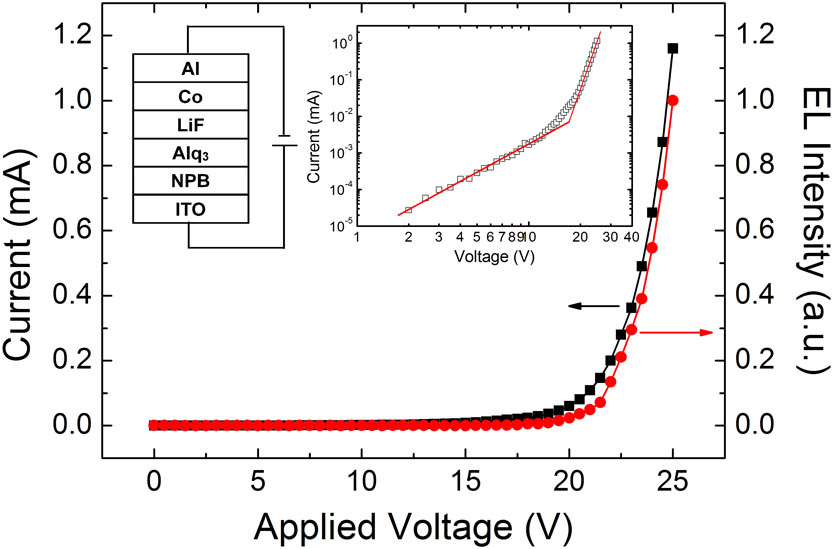
Figure 1.EL intensity-voltage and current-voltage characteristics of the devices with Co thickness of 4 nm at 50 K. The device structure is schematically shown in the left inset, and the results fitted according to the power law are shown in the right inset.
The measurements were performed in a vacuumed optical cryostat that was placed in between the pole pieces of an electromagnet. The field was applied parallel to the device electrodes. A Keithley 238 apparatus was used as a constant bias voltage source. The emission was collected by a silicon detector, coupled with a Newport 1830-C optical power meter. The MC and MEL responses were measured at a constant applied voltage while sweeping the field . MC and MEL are defined as following: where is the current through the device. A vibrating sample magnetometer (VSM) was used to measure the magnetic hysteresis loops of the samples at room temperature.
Figure 1 shows the brightness-current-voltage characteristics of a typical device with the Co thickness of 4 nm at 50 K. The I-V curve and B-V curve are similar, showing the typical rectifying behavior of OLEDs. The turn-on voltage is about 18 V, which is much higher than that in conventional OLEDs, but close to the previous results of OLEDs with FM electrodes[2,3]. The large turn-on voltage () may partly result from the mismatch of energy levels between Co and [2,3]. As shown in the inset of Fig. 1, the I-V characteristics of the device are well described by the power law of . In the low-voltage region (below ), is 1.5, reflecting that the current mainly results from space-charge-limited conduction mode . However, in the high-voltage region (above ), dramatically increases to 12. The high power law dependence of the current on the voltage is the characteristic for the trapped-charge-limited current mode, indicating the presence of traps in the organic layer[9,10]. The traps possibly result from the penetration of Co clusters during the preparing process, leading to the increased turn-on voltage and relatively poor EL performance of OLEDs with FM electrodes. It suggests that improving the quality of the film forming and optimizing the device structure can be beneficial to the improved EL performance of magnetic OLEDs.
Figure 2 shows the MEL and MC characteristics of the sample at 50 K, with the applied bias voltage of 25 V. The device shows positive MEL and MC, about 4.35% and 1.67% (), respectively. These values are close to those obtained in typical conventional OLEDs. It is obvious that the MELs are much larger than the MCs. However, the MEL and MC have similar shapes, which can be well fitted with the modified empirical “non-Lorentzian” formula: MEL (MC) , where is applied magnetic field and is related to the magnitude of the hyperfine coupling strength; the value is 8.1 mT here. Similar phenomena have also been observed in conventional OLEDs without FM electrodes; however, the field dependence on MEL and MC has not been investigated in detail in the previous OLEDs with one FM electrode[1–7,11]. We thus conclude that the MFEs in the device have similar origins as those in OLEDs without FM electrodes. As we know, hyperfine coupling plays a very important role in organic devices due to the weak spin-orbit coupling, which could interconvert triplets into singlets and vice versa, while the applied magnetic field could change the intersystem conversion rate via Zeeman splitting, thus increasing the singlet/triplet ratio, resulting in the enhancement of the EL[1,12]. Moreover, the singlet excitons are more likely to be dissociated; thus, the increase of the singlet/triplet ratio causes more carriers that come from the dissociation, leading to the positive MC[1,12].
Figure 2.(a) MEL and (b) MC response of the device with the Co thickness of 4 nm under the bias voltage of 25 V at 50 K is plotted. Red solid lines show the non-Lorentzian line shape.
As shown in Fig. 3, the MEL and MC responses decreased accordingly with the increase of the voltage. MEL reaches the optimal values, about 5.81% at 21 V, then drops to about 3.64% at 26 V. The MC shows a similar trend, decreasing slightly from 1.96% (23 V) to 1.64% (26 V). Due to its unacceptable fluctuation, the MC values at low voltages (21 and 22 V) are absent fron the figure. The result is in good agreement with previous work, in which it monotonically decreases with the increase of the driving bias[11]. Similar experimental results are also observed in the device at different temperatures. In OLEDs, electrons and holes are injected from the electrodes and form excitons in the organic layer. With the increase of the applied voltage, more carriers are injected into the organic layer and form e-h pairs. However, only a small number of e-h pairs can contribute to the MFE due to the shorter e-h pair lifetime, resulting in the decrease of the EL and the current[13].
Figure 3.MEL and MC values as a function of bias voltage in the device under the applied field of 42 mT at 50 K.
The temperature dependence of the MEL was also investigated. As illustrated in Fig. 4, the MELs were measured under the field of 42 mT with the bias voltage of 25 V at several temperatures (50–250 K). Starting at 50 K, the MEL value increases with the rise of temperature, then shows a maximum at 200 K and decreases slightly as the temperature is further increased. It should be noted that a similar non-monotonic dependence on temperature has been reported for the MFE on photocurrents in organic materials[14]. As discussed in the above voltage dependence of MEL, the injected carriers and the e-h pair lifetime affect the MFE process. At low temperatures, the charge carrier injection and transport are improved in the OLEDs with the rise of the temperature due to the thermal-activated transport property of organic materials; thus, the number of e-h pairs that is affected by the magnetic field also increases, leading to the increase of MEL. However, with the further increase of the temperature, the lifetime of the e-h pairs rapidly decreases, resulting in the drop of MEL[13,14].
Figure 4.Temperature dependence of MEL in the device with the Co thickness of 4 nm under 25 V.
Figure 5 shows MEL and the turn-on voltage as a function of the Co thickness from 2 to 18 nm at 50 K, with the applied magnetic field of 42 mT and the bias voltage of 25 V. As shown in Fig. 5, the MEL first roughly increases and then decreases as the Co thickness increases, reaching the optimal value in the sample with the Co thickness of 10 nm, about 7.83%. Moreover, the turn-on voltage of the dependence on the Co thickness is a little different from the MEL. With the increase of the Co thickness, the turn-on voltage rises from 17.5 V (2 nm) to 21 V (10 nm) and then fluctuates around 21 V.
Figure 5.MEL and turn-on voltage as a function of Co thickness in the devices under the applied field of 42 mT at 50 K.
Due to the deposition of the metal on top of a soft material, the metal atoms inevitably diffuse and penetrate into the underneath organic layer, forming the so-called “ill-defined layer,” of which the thickness varies from several nanometers to hundreds of nanometers[15]. To reduce the metal penetration, a thin LiF buffer layer was inserted between the organic layer and the upper Co electrode[8,15]. At the beginning of the deposition, discrete Co clusters drop on the surface of the layer and partly penetrate into the layer. As the Co is deposited, more and more magnetic clusters aggregate and begin to connect each other. They then percolate to form a network and finally form a continuous layer. According to the previous reports, the nominal threshold thickness is about several nanometers depending on the fabrication condition[6,16]. Due to the high work function of Co (5.0 eV), the injection of electrons from Co is more difficult than that from Al (4.2 eV)[17]. Therefore, with the increase of the nominal thickness, the Co coverage is improved accordingly, resulting in an increasing turn-on voltage. When the continuing Co layer is formed (about 10 nm), the turn-on voltage will no longer go up.
As for MEL dependence on Co thickness, we can explain it with the spin-polarized injection mechanism. With the increase of Co’s nominal thickness, an increasing number of Co clusters appears at the interface, bringing about the increase of the injecting spin-polarized electrons, thus resulting in the enhancement of MEL. It has previously been shown that the ill-defined Co layers or Co clusters can realize efficient spin-polarized injecting and improve the injection of the carriers, thus enhancing the EL[6,16], and the traps formed by Co penetration can also be beneficial to the EL[10]. Meanwhile, the exciton could be dissociated when the charge carrier concentration is much higher in the organic materials at the high-electric field. Thus, for the same bias voltage, the higher turn-on voltage in thicker Co samples results in less current density and a higher MEL. With the further increase of Co thickness, a continuous Co layer is formed, and the contact specific surface area of Co decreases accordingly, lowering the spin-polarized injection and leading to the decrease of MEL. The above non-monotonic Co thickness dependence of MEL is substantially consistent with previous reports[6]. Therefore, the optimal microstructure of magnetic OLEDs is a key factor to obtaining large MELs. Our MEL results are a little bit below the newly reported value (12%)[5]. In order to obtain better MELs, optimizing the microstructure and using a high spin-polarized electrode is suggested in follow-up studies. Moreover, a minor peak of the MEL curve also can be observed at 4 nm, which is possibly related to the microstructural characteristic of the sample. Further investigation is needed to clarify it.
Figure 6 shows the normalized magnetic hysteresis loops for samples with different Co thicknesses at room temperature. In the in-plane configuration, the applied field is parallel to the Co electrode. For the samples with a thin Co nominal thickness (below 10 nm), the hysteresis loops show a superparamagnetic nature, namely showing nonhysteresis and isotropic characteristics. This indicates the granular characteristic of the Co clusters in the ill-defined layer[18,19]. With the increase of the Co thickness, the in-plane magnetization of the sample is easier to saturate, indicating the gradual formation of the continuous layer. The VSM results are consistent with the possible microstructure characteristics of the samples.
Figure 6.Normalized hysteresis loops for the samples with different Co thicknesses.
In conclusion, we fabricate a series of OLEDs with different thicknesses of Co and measured the MELs and MCs at various temperatures. The positive MEL and the MC are observed in the samples, showing a non-Lorentzian line shape. The MEL and MC dependence on the voltage, temperature, and Co thickness are investigated, and the electron-hole pair model and the spin-polarized injection mechanism are used to explain the experimental phenomena.
Junqiang Shao, Xueting Yuan, Zelin Mu, Gang Ni. Magnetic field effects in organic light-emitting diodes with Co electrode[J]. Chinese Optics Letters, 2016, 14(6): 062501