Abstract
In recent years, the nanostructure for solar cells have attracted considerable attention from scientists as a result of a promising candidate for low cost devices. In this work, quantum dots sensitized solar cells with effective performance based on a co-sensitized (or ) nanocrystal, which was made by successive ionic layer absorption and reaction, are discussed. The optical, physical, chemical, and photovoltaic properties of quantum dots sensitized solar cells were sensitized to and dopants. Therefore, the short current () of the quantum dot sensitized solar cells is boosted dramatically from for pure CdSe nanoparticles to for ions and for ions. Actually, metal dopant extended the band gap of pure CdSe nanoparticles, reduced recombination, enhanced the efficiency of devices, and improved the charge transfer and collection. In addition, and dopants rose to the level of the conduction band of pure CdSe nanoparticles, which leads to the reduction of the charge recombination, enhances the light-harvesting efficiency, and improves the charge diffusion and collection. The results also were confirmed by the obtained experimental data of photoluminescence decay and electrochemical impedance spectroscopy.For decades, quantum dot sensitized solar cells (QDSSCs) based on quantum dots (QDs) have been of considerable interest as promising candidates to replace the dye sensitized solar cells (DSSCs) because QDs have potential functions, such as a high extinction coefficient, tunable bandgaps, a large intrinsic dipole moment, generation of multiple excitons[1], and low processing cost compared to organic dyes[2,3]. The QDs were used in QDSSCs as sensitizers that include PbS[4,5], PbSeS[6], CdS[7], CdSe[8], CdTe[9], and ZnS[10]. The highest efficiency, which was achieved by Jara et al., was approximately 2.51% for [11], because the electrons in the conduction band (CB) of the QDs move to the electrolyte and recombine or get blocked. Moverover, tandem multilayers can increase the power conversion efficiency in the QDSSCs. For instance, Jung et al. studied the QDSSCs based on the tandem multilayers, and the power conversion efficiency was about 1.47%[12,13]. This photovoltaic performance was higher than those of the lonely CdS and QDs. However, the efficiency was still minor because of the increased combination processes at the surface and plenty of electrons moving to the electrolyte.
In order to boost the conversion efficiency of photovoltaics, /CdS/CdSe/ZnS multiplayers have been studied to improve the short current () density of solar cells[14,15]. As a result, photoanodes can absorb a large amount of photons from the UV to the visible region. Furthermore, the ZnS coating forms a potential barrier between the QDs and the electrolyte, blocking the electrons in the CB transfer from the QDs to the electrolyte and reducing the defect states in the QDs[16]. In recent years, researchers reported the result of metals doped on nanoparticles, such as on PbS[17] and on CdS[18]. As a result, it could boost the density and efficiency of solar cells as compared with pure CdS and PbS QDs and CdSe QDs due to enhancing the light harvesting, generation, collection, and injection of the excited electrons between nanoparticles and film[19,20]. The performance of CdSe QDSSCs is much higher than that of the sulfide QDSSCs[21–25]. Therefore, metal ions doped on pure CdSe QDs can be a useful way for high efficiency QDSSCs[26,27].
As mentioned above, QDSSCs based on metal ions doped on CdSe nanoparticles with the different compositions of the and the are achieved by successive ionic layer adsorption and reation (SILAR). Moreover, the significant effects of the X dopant on optical, physical, chemical, and photovoltaic properties of films can be studied by the UV-visible (UV-Vis) spectra and Tauc plots to determine the band gap, CB, and valence band (VB) positions of metal ions. In the same way, the dynamic processes of QDSSCs are also studied through photoluminescence (PL) decay and electrochemical impedance spectra (EIS).
Sign up for Chinese Optics Letters TOC. Get the latest issue of Chinese Optics Letters delivered right to you!Sign up now
In this experiment, a fluorine-doped tin oxide (FTO) glass substrate with sheet resistance was used for the photoanode and the counter electrode. First, the FTO substrate was cleaned in ethanol for 30 min by ultrasonics, followed by deionized (DI) water for 15 min. The nanoporous film was made on the well-cleaned substrate by the print method followed by sintering at 500°C for 30 min. film: film was dipped into a ethanol solution (0.1 M, 1 M = 1 mol/L) for 5 min, rinsed with ethanol, and dried, then successively dipped into a methanol solution (0.1 M) for another 5 min, rinsed with methanol, and dried. The two-step dipping procedure was termed as one SILAR cycle. The process was repeated for three times, and the obtained film decorated with CdS QDs was named as the film[28–31]. film: film was dipped into a mixed and ethanol solution for 5 min, rinsed with ethanol, and dried, then successively dipped into a Se source methanol solution for 5 min, rinsed with methanol, and dried. The two-step dipping procedure was termed as one SILAR cycle. The process was repeated for three times as with representing the -doped molar concentration at 5%, 10%, 20%, 30%, and 40%. film: Sodium selenosulphate () 0.3 M was used as the Se source for SILAR. The aqueous solution was prepared by refluxing Se (0.3 M) in an aqueous solution of (0.6 M) and NaOH (1M) at 70°C for about 7 h. To accommodate the doping of the ion, relevant molar concentrations of 0.1 mM, 0.2 mM, 0.3 mM, 0.4 mM, and 0.5 mM of were mixed with a anion source. The SILAR process of CdSe and -doped CdSe QDs was similar to that of CdS, except that 15 min and 50°C were required for dipping the film in the aqueous solution. Different electrodes were named as with representing the -doped molar concentration and number of the SILAR cycle, respectively. Finally, the electrode was coated with a ZnS passivation layer by dipping alternately into 0.1 M and 0.1 M DI water solution for 5 min each. This process was repeated twice to get the optimal thickness[28–31].
A polysulfide solution was made by dissolving 0.5 M , 0.2 M S, and 0.2 M KCl in DI water/methanol (7:3 by volume). The counter electrode was synthesized through chemical bath deposition according to Ref. [32]. Briefly, 0.24 g was dissolved in 60 mL DI in a glass bottle. was bubbled through the water for 10 min to remove the dissolved oxygen from the system. Then, 0.37 g was mixed in the solution, and the color turned to light green. Afterwards, a clean FTO glass was immersed in the solution with its conductive surface facing down and had an angle against the wall. The system was then settled in the water bath of 90°C and kept for 1 h. The crystal would directly grow onto the conductive surface of the FTO glass. Finally, the as-prepared -coated FTO glass sample was rinsed with DI water and dried in air. The post-heating treatment was carried out in an atmosphere at 200°C for 30 min.
The morphologies of the samples were investigated using scanning electron microscopy (SEM). The crystal structure was analyzed using an X-ray diffractometer (Philips, PANalytical X’Pert, radiation). The absorption properties of the samples were investigated using a diffuse reflectance UV–Vis spectrometer (JASCO V-670). Photocurrent–voltage measurements were performed on a Keithley 2400 source meter using simulated air mass (AM) 1.5 sunlight with an output power of produced by a solar simulator (Solarena, Sweden). The EIS was carried out with the use of an impedance analyzer (ZAHNER CIMPS). The PL spectra were measured by an excitation wavelength of 430 nm at room temperature using a Shimadzu luminescence spectrometer RF-5301PC.
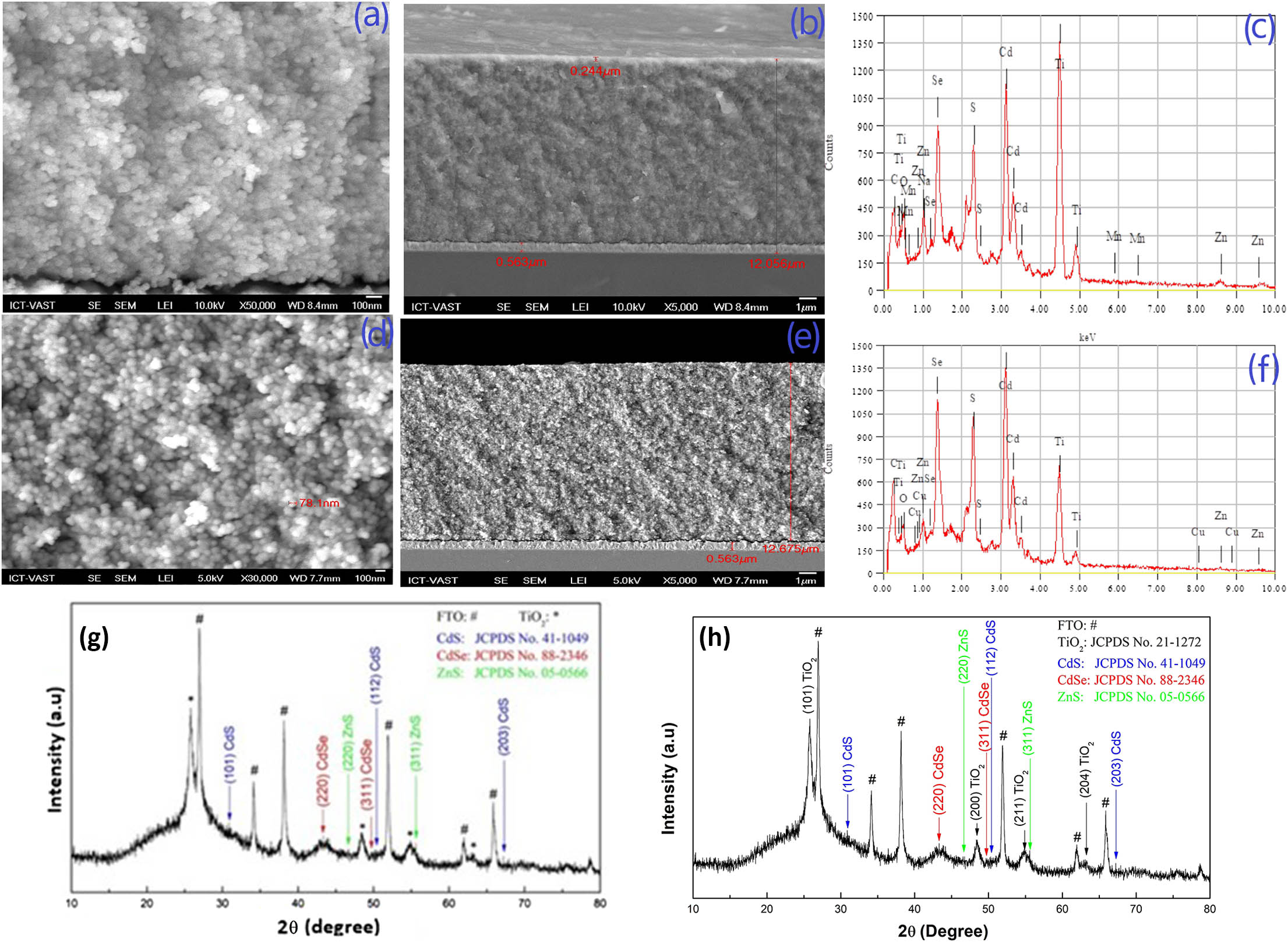
As far as previous work is concerned, the nanoparticles were deposited on the FTO substrate[33]. Therefore, we only discussed the details based on the deposition of CdS, CdSe:X nanoparticles on the . The typical field emission SEM (FE-SEM) images of co-sensitized (or ) show that the mood surface morphology [Figs. 1(a) and 1(d), respectively] and nanoparticles are nearly spherical with an average cluster size of over 70 nm, which agrees well with the X-ray diffraction (XRD) analysis. Besides, the thicknesses of photoanode films are determined as approximately 12.056 μm (, , : 720 nm, and ZnS: 120 nm) for and 12.675 μm (FTO: 0.563 μm, , : 615 nm, and ZnS: 120 nm) for by cross-sections [Figs. 1(b) and 1(e), respectively]. The compositional energy dispersive X-ray (EDX) analysis of the CdSe:X was shown in Figs. 1(c) and 1(f), and the experimental data was recorded in Tables 1 and 2, which proves the presence of and dopants in photoanodes. As can be seen from Figs. 1(g) and 1(h), they are the same structures of , CdS, and (). It is immediately obvious that the XRD patterns of and appear at the peaks at the 47.4° and 55.7° positions, corresponding to the (200) and (111) planes, which indicates an upstanding ZnS blend. It is completely suitable with the Joint Committee on Powder Diffraction Standards (JCPDS) No. 05-5666. It also shows that the peaks at the 43.3° and 50.0° positions correspond to the (220) and (311) planes of the CdSe zinc blend (JCPDS No. 88-2346), and the peaks at 30.7°, 50.6°, and 67.2° correspond to the (101), (112), and (203) planes of the CdS zinc blend (JCPDS No. 41-1019), respectively. Finally, the left peaks of XRD characterize the anatase (JCPDS No. 21-1272). This implies that CdS, , and ZnS nanoparticles have been absorbed on films.
| Elements | Energy (keV) | Mass fraction (%) | Atom fraction (%) |
|---|
| C | K | 0.277 | 5.09 | 24.37 |
| O | K | 0.525 | 0.77 | 2.78 |
| S | K | 2.307 | 8.25 | 14.78 |
| Ti | K | 4.508 | 13.85 | 16.62 |
| Cu | K | 8.040 | 0.45 | 0.41 |
| Zn | K | 8.630 | 0.66 | 0.58 |
| Se | L | 1.379 | 19.39 | 14.11 |
| Cd | L | 3.133 | 51.53 | 26.35 |
Table 1. Composition of
| Elements | Energy (keV) | Mass fraction (%) | Atom fraction (%) |
|---|
| C | K | 0.277 | 1.00 | 4.31 |
| O | K | 0.525 | 1.82 | 5.91 |
| Na | K | 1.041 | 1.07 | 2.42 |
| Al | K | 1.486 | 1.10 | 2.13 |
| Si | K | 1.739 | 0.83 | 1.54 |
| S | K | 2.307 | 7.38 | 11.96 |
| Ti | K | 4.508 | 50.71 | 55.04 |
| Cd | L | 3.133 | 36.09 | 16.69 |
Table 2. Composition of

Figure 1.(a), (d) FE-SEM image at 100 nm, (b), (e) cross-section at 1 μm, and (c), (f) EDX pattern of co-sensitized (or ). (g), (h) XRD patterns of co-sensitized (or ) QDSSCs.
In QDSSCs, a band alignment of nanoparticles in an anode is quite necessary for us to explain the diffraction and movement of excited electrons in CB levels of a semiconductor. The band gap of CdSe bulk, which can be absorbed in the visible region, is approximately 1.76 eV[33], but the CB of CdSe becomes lower than that of . Therefore, injection of the excited electrons into film becomes hard. On the other hand, the CB of CdS bulk is higher than that of , which is the driving force, making the movement of the excited electrons to easier[34]. Co-sensitized CdS/CdSe can significantly improve the performance of QDSSCs[34,35]. In addition, Lee and co-workers said that the Fermi energy of CdSe nanoparticles shifted to above, while that of CdS nanoparticles shifted down, as CdS/CdSe co-sensitized to make the structure[24]. Therefore, the excited electrons are able to easily transfer from CdSe, CdS nanoparticles to .
Moreover, the CB and VB positions of CdS and CdSe nanoparticles can be determined by the Tauc equation to demonstrate the abovementioned. The CB and VB of materials can be calculated if the electron affinity energy and the ionization energy are known. Similarly, the CB, VB of CdS and CdSe can be determined by the Tauc equation as follows[36–38]: where with is the CB potential, is a given constant equal of 4.5 eV[37–39], is an energy parameter and depends on the elements of composition, and is the band gap of materials. and are the electron affinity energy and the ionization energy of CdS, CdSe, respectively. The values of and for Cd, S, and Se are 0, 2.077, 2.020 eV and 8.99, 10.36, 9.75 eV, respectively. Finally, the calculated parameters are listed in Table 3.
| Materials | Eg(eV) | X(eV) | ECB(eV) | EVB(eV) |
|---|
| Pure CdSe | 2.03 | 5.102 | −4.08 | −6.11 |
| CdSe:Mn2+ (20%) | 1.75 | 4.620 | −3.74 | −5.49 |
| CdSe:Cu2+ (0.3%) | 1.73 | 4.913 | −4.05 | −5.78 |
Table 3. , CB, and VB Positions of the Co-sensitized (or ) Calculated by the Tauc equation and UV-Vis Spectra
Looking at Fig. 2(a), it is immediately obvious that the absorbances of the and the were not only much higher than that of the pure CdSe, but also significantly shifted towards the long wavelength region (red shift). For this reason, the increased absorbance of photoanodes can be contributed to the dopant in CdSe nanoparticles. Besides, this also implies that the energy level of the dopant is made in the band gap of the pure CdSe nanoparticles, corresponding to the state of the dopant[39–41]. In brief, the presence of in CdSe nanoparticles is not only shifting towards the long wavelength region, but also the enhanced absorbance of films leading to the high performance QDSSCs.
Figure 2.(a) UV-Vis spectra and (b) vs (hν) curves of the pure CdS/CdSe and co-sensitized (or ) QDSSCs.
The of CdS, (or ) obtained from UV-Vis spectra and the CB and VB positions of CdS, and (or ) can be determined by Tauc Eq. (1) [Fig. 2(b) and Table 3]. The of the and nanocrystals are calculated with values of 1.75 and 1.73 eV, respectively, which are smaller than that (2.03 eV) of pure CdSe nanoparticles. Therefore, the presence of in CdSe nanoparticles could reduce of pure CdSe, which enhances the efficiency of high harvesting. Conversely, the CB and VB levels of the CdSe: and CdSe: are estimated and listed in Table 3 with values of and , respectively, which are higher than both that () of pure CdSe and that () of the CdS nanocrystal. As a result, the dopant in CdSe nanoparticles facilitates the transfer of the electrons from CdSe, CdS nanoparticles to .
Figure 3(a) shows the excited state electron radiative decay of film loaded with the , , and pure CdSe nanocrystals corresponding to 200, 203, and 206.5 ns, respectively. It is obvious that the emission decays of the and nanocrystals are longer than that of the pure CdSe, which indicates that the PL lifetime of pure CdSe nanoparticles can be slightly shortened by the dopant. In that case, there is a significant rise of density (Table 4) because of the increase of the injection kinetics of photogenerated electrons in nanoparticles. This result also shows a growth of the CB of , which is completely suitable with result of the UV-Vis spectra and references[42–45].
| Anodes | JSC (mA/cm2) | FF | VOC (V) | η (%) | RS (Ω) | RCE (Ω) | Rct (Ω) | Cμ (μF) |
|---|
| Pure CdSe | 12.351 | 0.382 | 0.417 | 1.96 | 20.25 | 630.5 | 194.8 | 12.25 |
| CdSe:Mn2+ (20%) | 18.990 | 0.381 | 0.520 | 3.77 | 17.05 | 204.5 | 24.65 | 120.9 |
| CdSe:Cu2+ (0.3%) | 19.915 | 0.421 | 0.503 | 4.22 | 19.29 | 254.4 | 8.681 | 160.5 |
Table 4. Values of J-V Curves and Electrochemical Impedance Spectra of the Pure CdS/CdSe and Co-sensitized (or ) QDSSCs
Figure 3.(a) PL decays and (b) photocurrent density–voltage (J-V) curves of the pure CdS/CdSe and co-sensitized (or ) QDSSCs.
As far as the introduction part is concerned, QDSSCs based on co-sensitized (or ) with a concentration of at 20% and at 0.2% obtained the best optical properties. Therefore, QDSSCs were prepared and compared as concentrations of at 30% and at 0.3%. Figure 3(b) illustrates the J-V characteristics for the QDSSCs based on the different photoanodes under illumination of one sun (AM 1.5, ), and the parameters are listed in Table 4. It is clear that the QDSSCs based on (20%) and (0.3%) exhibit higher performance: , , , and , and , , , and , respectively. As can be expected, there was a sharp increase of the current density from 12.351 to 18.99 and after ions were doped on the CdSe nanoparticles, which is a main cause of the enhanced performance in the QDSSCs. The efficiency of the QDSSCs is improved as is doped on CdSe nanoparticles by the following reasons: firstly, an increase of light harvesting, charge transfer, and charge collection; secondly, the lifetime of co-sensitized (or ) is longer than that of pure CdS/CdSe nanoparticles. In addition, there was a rapid growth of efficiency from 1.96% to 3.77% and 4.22%.
The band alignments of (or ) and /CdS/CdSe are illustrated in Fig. 4(a), and the value parameters are calculated in Table 3. It is obvious that both the CB and VB positions of and are higher than those of both pure CdSe and CdS nanoparticles. Therefore, the () tandem structure is made by doped on pure CdSe nanoparticles. This implies that it facilitates the transfer of the electrons from CdSe nanoparticles to CdS and , making it easier to improve the performance of the QDSSCs. Moreover, the energy levels of dopants appear in the band gap and the VB of nearly pure CdSe nanoparticles for at about 0.31 and 1.73 eV, and the VB of nearly pure CdSe nanoparticles for at approximately 0.38 and 1.8 eV, respectively. These results are definitely suitable for Refs. [46–51].
Figure 4.(a) Schematic diagram for the band alignment in ( or ) QDSSCs and (b) Nyquist curves of pure CdSe and CdSe:X-QDSSCs.
In order to illustrate the dynamic processes in the QDSSCs, the EIS of the (or ) photoanodes are measured. Fig. 4(b) shows the EIS characteristics for the QDSSCs based on the different photoanodes and parameters that are listed in Table 4. Rs is a set of resistance to the charge transfer at Ag/FTO/ front contact and Ag/FTO/ back contact; Rs values are obtained at about for the best photoanodes. The result shows that the applied technique is strongly affected. The is the resistance at the /electrolyte and the interfaces. The is the resistance against the electron diffusion in , the charge recombination resistance at the /QDs/electrolyte interface, and against the inside diffusion in the electrolyte (Zw).
Compared with CdSe:, a semicircle of a pure CdSe nanoparticle is largely extended, corresponding to the largest () resistance, which is approximately (), while the is the smallest (12.25 μF) and the lifetime is the shortest (200 ns). Besides, there was the diminishing of semicircles as X was doped on pure CdSe nanoparticles, and the () resistances of and decreased dramatically from 194.8 to 24.65 and (from 630.5 to 204.5 and ), while there was an upward trend of the from 12.25 to 120 and 160.5 μF, respectively. It is noticeable that the ions doped on pure CdSe nanoparticles can enhance the light harvesting, generation, collection, and injection of the excited electrons between nanoparticles and film. It is completely suitable with that of the UV-Vis [the CB and VB levels of the () are estimated and listed in Table 3 with values of (), which are higher than both that of pure CdSe () and that of CdS ()].
The () nanocrystals were synthesized by SILAR. It was found that the () nanocrystals adopt a blended structure over all of the compositions, and the ternary () nanocrystals with tunable band gap properties extend the band edge of the optical light absorption from 500 to 610 nm compared to the pure CdSe. The QDSSCs based on the () anodes were successfully prepared, which exhibit the high performance: , , , and (, , and ), respectively. This result shows that the () ions doped on pure CdSe nanoparticles can increase the light harvesting to produce more excitons, making a fast electron transfer at ()/ZnS/electrolyte interfaces, and the reduced recombination in the QDSSCs as ZnS coating protected nanoparticles. Moreover, the () dopant raises the CB levels of CdSe nanoparticles, which are higher than that of CdS nanoparticles, accelerating the exciton injection kinetics in the QDSSCs.
References
[1] M. C. Beard. J. Phys. Chem. Lett., 2, 1282(2011).
[2] P. V. Kamat. J. Phys. Chem. C, 112, 18737(2008).
[3] A. Nozik. J. Phys. E, 14, 115(2002).
[4] S. S. Mali, S. K. Desai, S. S. Kalagi, C. A. Betty, P. N. Bhosale, R. S. Devan, Y.-R. R. Mad, P. S. Patila. Dalton Trans., 41, 6130(2012).
[5] J. Jiao, Z.-J. Zhou, W.-H. Zhou, S.-X. Wu. Mater. Sci. Semicond. Process, 16, 435(2013).
[6] N. P. Benehkohal, V. González-Pedro, P. P. Boix, S. Chavhan, R. Tena-Zaera, G. P. Demopoulos, I. Mora-Seró. J. Phys. Chem., 1, 16391(2012).
[7] Q. Zhang, Y. Zhang, S. Huang, X. Huang, Y. Luo, Q. Meng, D. Li. Electrochem. Commun., 12, 327(2010).
[8] V. González-Pedro, X. Xu, I. Mora-Seró, J. Bisquert. ACS Nano, 4, 5783(2010).
[9] Z. Yang, H.-T. Chang. Sol. Energy Mater. Sol. Cells, 94, 2046(2010).
[10] N. Balisa, V. Dracopoulos, K. Bourikas, P. Lianos. Electrochim. Acta, 91, 246(2013).
[11] D. H. Jara, S. Joon Yoon, K. G. Stamplecoskie, P. V. Kamat. Chemi. Mater., 26, 7221(2014).
[12] S. Woo Jung, J.-H. Kim, H. Kim, C.-J. Choi, K.-S. Ahn. J. Curr. Appl. Phys., 12, 1459(2012).
[13] T. R. Ravindran, A. K. Arora, B. Balamuruga, B. R. Mehta. Nanostruct. Mater., 11, 603(1999).
[14] T. Lopez-Luke, A. Wolcott, L.-P. Xu, S. Chen, Z. Wen, J. Li, E. D. L. Rosa, J. Z. Zhang. J. Phys. Chem. C, 112, 1282(2008).
[15] I. Mora-Sero, S. Gimenez, T. Moehl, F. Fabregat-Santiago, T. Lana-Villareal, R. Gomez, J. Bisquert. Nanotechnology, 19, 424007(2008).
[16] Q. Shen, J. Kobayashi, L. J. Diguna, T. Toyoda. J. Appl. Phys., 103, 084304(2008).
[17] J.-W. Lee, D.-Y. Son, T. K. Ahn, H.-W. Shin, I. Y. Kim, S.-J. Hwang, M. J. Ko, S. Sul, H. Han, N.-G. Park. Sci. Rep., 3, 1050(2013).
[18] P. K. Santra, P. V. Kamat. J. Am. Chem. Soc., 134, 2508(2012).
[19] L. Zhu, T. X. Pan, Z. Sun. ACS Appl. Mater. Interfaces, 3, 3146(2011).
[20] Y. H. Lee, S. H. Im, J. A. Chang, J. H. Lee, S. I. Seok. Org. Electron., 13, 975(2012).
[21] M. A. Hossain, J. R. Jennings, C. Shen, J. H. Pan, Z. Y. Koh, N. Mathews, Q. Wang. J. Mater. Chem., 22, 16235(2012).
[22] Z. Pan, K. Zhao, J. Wang, H. Zhang, Y. Feng, X. Zhong. ACS Nano, 7, 5215(2013).
[23] J. G. Radich, N. R. Peeples, P. K. Santra, P. V. Kamat. J. Phys. Chem. C, 118, 16463(2014).
[24] J. Wang, I. Mora-Sero, Z. Pan, K. Zhao, H. Zhang, Y. Feng, G. Yang, X. Zhong, J. Bisquert. J. Am. Chem. Soc., 135, 15913(2013).
[25] K. Yan, L. Zhang, J. Qiu, Y. Qiu, Z. Zhu, J. Wang, S. Yang. J. Am. Chem. Soc., 135, 9531(2013).
[26] Q. Dai, E. M. Sabio, W. Wang, J. Tang. Appl. Phys. Lett., 104, 183901(2014).
[27] T. Debnath, P. Maity, S. Maiti, H. N. Ghosh. J. Phys. Chem. Lett., 5, 2836(2014).
[28] Y. L. Le, Y. S. Lo. Adv. Funct. Mater., 19, 604(2009).
[29] Y. L. Xie. Electrochim. Acta, 105, 137(2013).
[30] C. Xing, Y. Zhang, W. Yan, L. Guo. Int. J. Hydrogen Energy, 31, 2018(2006).
[31] M. Askari, N. Soltani, E. Saion, W. M. M. Yunus, M. H. Erfani, M. Dorostkar. Superlattices Microstruct., 81, 193(2015).
[32] A. S. Hassanien, A. A. Akl. Superlattices Microstruct., 89, 153-169(2015).
[33] H. T. Tung, N. T. Thao, L. Q. Vinh. Int. J. Photoenergy, 8, 8545207(2018).
[34] B. S. Bhupendra, S. Jana, N. Pradhan. J. Am. Chem. Soc., 133, 1007(2011).
[35] M. P. A. Muthalif, Y. S. Lee, C. D. Sunesh, H. J. Kim, Y. Choe. Appl. Surf. Sci., 396, 582(2016).
[36] S. K. Niladri, D. D. Sarma, R. M. Kadam, N. Pradhan. J. Phys. Chem. Lett., 1, 2863(2010).
[37] C. Corrado, Y. Jiang, F. Oba, M. Kozina, F. Bridges, J. Z. Zhang. J. Phys. Chem. A, 113, 3830(2009).
[38] P. Mandal, S. S. Talwar, S. S. Major, R. S. Srinivasa. J. Chem. Phys., 128, 114703(2008).
[39] N. Pradhan, D. Goorskey, J. Thessing, X. Peng. J. Am. Chem. Soc., 127, 17586(2005).
[40] R. Xie, X. Peng. J. Am. Chem. Soc., 131, 10645(2009).
[41] R. Beaulac, S. T. Ochsenbein, D. R. Gamelin. Nanocrystal Quantum Dots(2010).
[42] A. A. Bol, J. Ferwerda, J. A. Bergwerff, A. Meijerink. J. Lumin., 99, 325(2002).
[43] C. Gan, Y. Zhang, D. Battaglia, X. Peng, M. Xiao. Appl. Phys. Lett., 92, 241111(2008).
[44] S. Jana, B. B. Srivastava, S. Acharya, P. K. Santra, N. R. Jana, D. D. Sarma, N. Pradhan. Chem. Commun., 46, 2853(2010).
[45] B. B. Srivastava, S. Jana, N. S. Karan, S. Paria, N. R. Jana, D. D. Sarma, N. Pradhan. J. Phys. Chem. Lett., 1, 1454(2010).
[46] M. P. A. Muthalif, Y. S. Lee, C. D. Sunesh, H. J. Kim, Y. Choe. Appl. Surf. Sci., 396, 582(2016).
[47] T. H. Thanh, V. L. Quang, H. T. Dat. J. Nanomater., 9806386(2016).
[48] T. T. Ha, C. H. Chi, N. Vy, N. T. Thoa, T. D. Huynh, Q. V. Lam. Environ. Prog. Sustainable Energy, 34, 1774(2015).
[49] T. H. Thanh, V. L. Quang, D. H. Thanh. Sol. Energy Mater. Sol. Cells, 143, 269(2015).
[50] T. H. Thanh, L. Q. Vinh, H. T. Dat. Braz. J. Phys., 44, 746(2014).
[51] Y. F. Xu, W. Q. Wu, H. S. Rao, H. Y. Chen, D. B. Kuang, C. Y. Su. Nano Energy, 11, 621(2014).