1Shaanxi Key Laboratory of Optical Information Technology, School of Science, Northwestern Polytechnical University, Xi’an 710072, China
2State Key Laboratory of Transient Optics and Photonics, Xi’an Institute of Optics and Precision Mechanics, Chinese Academy of Sciences, Xi’an 710119, China
3Department of Electronic Information Engineering, Nanchang University, Nanchang 330031, China
We present the spatial resolution estimation methods for a photon counting system with a Vernier anode. A limiting resolution model is provided according to discussions of surface encoding structure and quantized noise. The limiting resolution of a Vernier anode is revealed to be significantly higher than that of a microchannel plate. The relationship between the actual spatial resolution and equivalent noise charge of a detector is established by noise analysis and photon position reconstruction. The theoretical results are demonstrated to be in good agreement with the experimental results for a 1.2 mm pitch Vernier anode.
Position[1–4] and arrival time[5–8] recordings of single photons can be achieved by photon counting detection, which realizes ultra-weak radiation imaging with high spatial and time resolutions. Thus, photon counting imagers have been widely used in many important fields such as space detection, astronomy, biomedicine, nuclear physics, quantum key distribution (QKD), photon counting microscopy, etc.[8–13]. The previous work from Lapington et al. reported a Vernier-based imager with a spatial resolution of FWHM result, near to the pore size of microchannel plates (MCPs), which reveals that a Vernier structure determined spatial resolution can exceed the limit of an MCP pore size by structure optimization and readout noise suppression[14,15]. However, the relationship between spatial resolution and the anode encoding structure with or without readout noise is still unclear. In other words, the estimation models of the limiting resolution determined by the encoding structure and the actual spatial resolution determined by readout noise are not established.
In this Letter, we provide the estimation methods of the limiting resolution and the actual spatial resolution. The influence factors of spatial resolution (including the limiting and actual resolutions) have been analyzed. The limiting resolution model is deduced by calculations of the encoding structure and the charge cloud on a Vernier anode. The inner relationship between the actual spatial resolution and the normalized noise characterized by the equivalent noise charge (ENC) has been revealed within a low noise range by noise analysis during the decoding process. The influence mechanism of the noise and anode structure on spatial resolution can be well understood using this model. Additionally, the point spread function (PSF)[16,17] for image super-resolution at low light illumination may be well characterized by using the resolution estimation model.
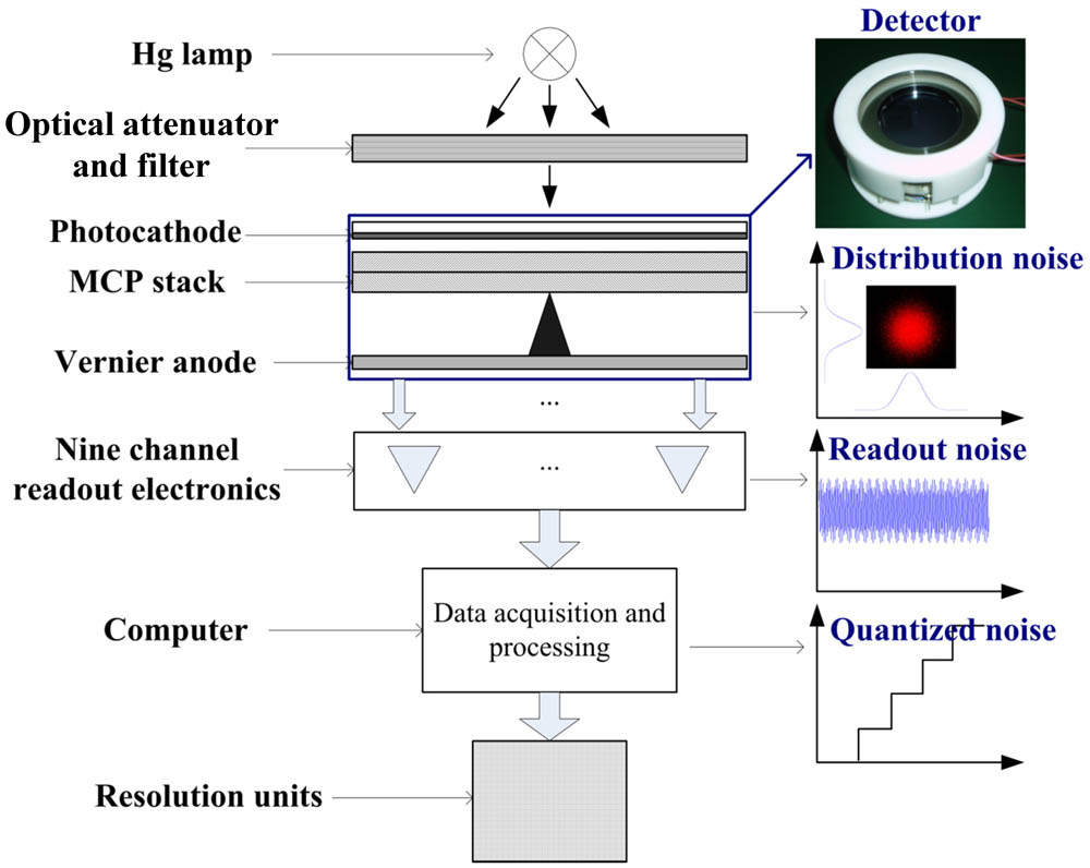
A photon counting imaging system based on a Vernier anode usually consists of the detector, the readout circuit, and the data acquisition and decoding subsystem[1–4]. The detector consists of an input window, photocathode, MCP, Vernier anode, vacuum packaging shell, etc. Figure 1 shows a typical photon counting imaging system based on a Vernier anode showing noise sources. The working principle can refer to Refs. [3,14,15].
Sign up for Chinese Optics Letters TOC. Get the latest issue of Chinese Optics Letters delivered right to you!Sign up now
Figure 1.Sketch of the Vernier anode-based imaging system showing the distribution noise of the charge cloud, electronic noise, and quantized noise of the data acquisition subsystem.
For a Vernier anode-based imager, the noise sources can be divided into four types: input, detector, readout, and acquisition noises, as shown in Fig. 1. The input noise may come from the power supply, cosmic rays, photon counting fluctuation, etc. The noise sources of detector include photocathode thermal electron emission, electronic noise in MCPs, anode etching structure[1], charge cloud distribution, secondary electron emission on anode surface, charge coupling between electrodes, etc. The readout noise may consist of thermal and shot noise of the readout electronics, nonlinearity, and inconsistency of the amplifiers for nine signal channels. The acquisition noise mainly comes from the quantized error of the A/D converters (ADCs)[2].
Many types of noise can be eliminated or suppressed by noise suppression and low noise readout techniques except for quantized noise, which is determined by the limited bit width of ADCs. Thus, the limiting resolution is determined by the encoding structure of the anode, the pore size of the MCP, and quantized noise. The spatial resolution can be improved to approach the limiting resolution by structure optimization of the detector with low readout noise[15]. To estimate the limiting resolution, the relationship between the encoding structure and the charge cloud as well as the quantized error should be analyzed.
For limiting resolution estimation, the spatial resolution of the detector will be determined by the quantized noise due to the limited bit width of the ADCs and the encoding structure of the anode[2]. The Vernier anode generally contains many pitches, which can be divided into three triplets, as shown in Fig. 2(a). Each triplet can be divided into three electrodes. The electrodes are isolated by two sinusoidal isolating channels with the same amplitudes and a phase offset of within each triplet so that the widths of the electrodes have a phase offset of in the Vernier encoding pattern. According to the decoding algorithms of the Vernier anode[3,14], the electrode width can be expressed as , where is the pitch width and is the phase coordinate of the triplet.
Figure 2.(a) Schematic encoding structure of the Vernier anode covered by the charge cloud showing only 4 pitches, (b) an image of a practical two-dimensional Vernier anode with 1.2 mm pitch fabricated by laser etching, (c) the geometrical relationship between the charge cloud and the anode encoding structure within the charge cloud region; the periodic length of the sinusoidal isolating channel is much greater than the radius of the charge cloud so that the width variation of the electrode is approximately linear within the charge cloud area.
The charge quantity at the electrode output port is the sum of the corresponding electrodes within the charge cloud area, which is generally equivalent to the charge collected by the electrode at the centroid, as shown in Fig. 2(b). Thus, it is considered to calculate the collected charge of each corresponding electrode within the charge cloud. Figure 2(c) shows the corresponding electrodes covered by the charge cloud in which each electrode is approximated to be aligned within the charge cloud covering area because the periodic length of the sinusoidal isolating channel is much greater than the radius of the charge cloud. The widths of the electrodes around the charge cloud centroid have phase offsets proportional to the distance from the electrode to the charge cloud centroid along the y direction. According to the decoding algorithms[3,14], this can be expressed as where is the width of the electrode around the centroid, is the phase coordinate of the electrode at the centroid, and is the position of the incident photon. Here, is the electrode index around the centroid, defined by , as shown in Fig. 2(c). The parameter is the initial phase offset, and can be determined by where is the conversion wavelength of the electrode along the direction. For the area division pattern shown in Fig. 2(a), the total area covered by the charge cloud can be expressed as . Here, is the area of the electrode group within the charge cloud, and can be defined as , where (with ) is the number of pitches covered by half of the charge cloud, determined by , as shown in Fig. 2(c). Here, [] is the operation to get the maximum integer that is not larger than . Here, is the area of the element electrode among the electrode group within the charge cloud, which can be determined by where is the length of element electrode , as shown in Fig. 2(c), which can be determined by ( and , where is the radius of the charge cloud). The area microvariation of the electrode group is the sum of that of the element electrodes within the charge cloud region, as shown in Fig. 2(c). According to the integral mean value theorem, the area microvariation of the electrode group as a function of position (, ) can be expressed as where is the width microvariation of element electrode at . According to Eq. (1), the width microvariation of the element electrode at can be determined as a function of the phase microvariation (or phase deviation). Combined with Eq. (4), the area microvariation of the electrode group can be determined by
Here, the relationship between the phase deviation and the equivalent area deviation is established for a specific electrode. The relationships for other electrodes in a triplet have an offset of versus this electrode. One can see that the noise transmission is controlled and modulated by structure parameters of the Vernier anode and the charge cloud. Once the equivalent area deviation is determined, the limiting resolution can be obtained by the analysis of the quantized noise.
The charge cloud density complies with the Gaussian distribution: , where is the charge cloud density at the centroid, is the charge quantity of the charge cloud, and is the distance to the centroid[18,19]. Due to the symmetric distribution of the charge cloud, the charge at the electrode output port can be equivalent to that collected at the centroid with a charge density of . The relationship between the charge microvariation and the area microvariation of the electrode covered by the charge cloud can be simplified as . The parameter is defined as[2]where is the charge collected at the electrode output port. The relationship between the charge collected by the electrodes and the electrode area within the charge cloud can be established using this parameter.
The quantized noise is determined by the reference voltage and the bit width of the ADCs as well as the gain of the readout electronics, which can be expressed as[2]where is the feedback capacitor of the charge sensitive preamplifiers, is the reference voltage of the data acquisition system, is the bit width of the ADCs, and is the gain of the readout amplifiers. The charge deviation of the electrode group can be detected and distinguished only if the deviation is no less than , determined by the data acquisition subsystem.
According to Eq. (5), the phase deviation determined by one electrode contains the factor and seems to yield infinity at . However, a phase coordinate should be determined by three electrodes that have a phase offset of between each other according to the decoding algorithms[3,14]. Thus, the decoded phase coordinate also exhibits a high accuracy so that the resulting phase deviation will not be very large. So the resulting phase coordinate deviation should contain a factor instead of . Considering that three electrodes determine a phase coordinate in the decoding process, the phase coordinate deviation should include the phase deviations of three electrodes. Associating with Eq. (5), the phase coordinate deviation can be expressed as
Here, the factor represents the influence of decoding process on the resulting phase deviation. The limiting position deviation amplitude can be derived from the phase deviations according to the decoding algorithms, which can be expressed as where is the size of the Vernier anode and (a constant integer designing a parameter of the anode) is the coarse pixel number of the anode[3,15]. It indicates that the relationship between the limiting resolution and charge cloud radius is periodic for a specific anode pitch. One can see that the larger the gain of the readout electronics and coarse pixel number, and the smaller the anode size, the higher the limiting resolution can be achieved.
We calculated the limiting resolution according to Eqs. (8) and (9) using MATLAB 7.0, and obtained the relation between the limiting resolution and influence factors (charge cloud radius and pitch width) with , as shown in Fig. 3(a). The parameter setup is as follows: [4], , , , , and . One can see that the limiting resolution changes periodically when the charge cloud radius increases. This indicates that multiple optimal values can be chosen with for a corresponding pitch length . The limiting resolution is improved when the pitch width decreases with an approximate linear relationship.
Figure 3.The limiting resolution calculation results with a readout electronics gain of 31.6 dB, an MCP electron gain of , a feedback capacitor of the charge sensitive preamplifiers of 1 pF, a reference voltage of the data acquisition system of 1 V, a bit width of the ADCs of 12, an anode size of 30 mm, and a coarse pixel number of 4; (a) as a function of the pitch width and the charge cloud radius , (b) as a function of the phase coordinate with , and .
In order to investigate the phase coordinate dependence of the spatial resolution limit, the position deviation amplitudes were obtained at different phase coordinates by appending Gaussian noise to the encoding data and comparing the resulting positions. Figure 3(b) shows the relationship between the limiting resolution and the phase coordinate with , , and , where one can see that the limiting resolution fluctuates slightly and periodically when the phase coordinate changes, indicating .
Moreover, the spatial resolution of the anode imagers is also limited by the MCP, which divides the imaging surface into discrete positions. The MCP limited resolution is determined by the pore pitch of the MCPs, which can be expressed as[2]. Combined with the limiting spatial resolution determined by the quantized noise and anode structure, the total limiting resolution should be expressed as
The FWHM result of the limiting resolution can be expressed as: according to the Gaussian noise distribution. The limiting resolution is determined by the anode structure and the MCP pore size, and can be used to characterize the limiting resolving capability of the photon counting system with the Vernier anode. The actual spatial resolution will approach the limiting resolution by the readout noise suppression.
For the actual photon counting system, there is a large amount of noise that mainly comes from the readout electronics and the detector itself. Partition noise and electronic noise may be dominant among all types of noise[1,4]. Partition noise is caused by the photon counting fluctuation, which complies with the Poisson distribution. The noise level can be characterized by the ENC. The spatial resolution will be deduced theoretically by the noise transmission of the detection system, which can be expressed as[4]: . Here, is the ENC of the electrode. Generally, the electronic and partition noise levels are significantly larger than that of the quantized noise of the ADCs and the equivalent noise determined by the MCP pore size. Thus, the total noise level of the photon counting system for the general situation can be expressed in the ENC as where and are the electronic and partition noises, respectively. The actual experimental resolution results should be affected by large electronic and partition noises.
To estimate the photon position deviations as well as the corresponding noise level, we appended Gaussian noise to the simulation data matrix for which the original positions of the pixels are certain so that position deviation can be estimated, then we calculated the position deviations for the and directions to evaluate spatial resolution during the position decoding process. The data matrix appended noise can approximately simulate the situation of the experimental acquisition data matrix. The gain of the amplifiers can be estimated to be 17.5 dB for the data according to signal amplification of the collected charge with an MCP electron gain of and a total voltage sampled at the outputs of the amplifiers of [4]. Figure 4(a) shows the relationships between the spatial resolution FWHM and the ENC for the detectors with different values within a low noise range with , , and . One can see that there is an approximate linear relationship between the FWHM and the ENC. It can be expressed as where is the MCP electron gain and is the electron charge. The linear relation will change to be rational if the ENC changes within a large range[4]. The estimation results determined by Eq. (12) exhibit a higher resolution than that of the theoretical estimation obtained by noise transmission because the least square method in the position decoding and noise suppression techniques in the signal processing have been used to reduce the decoded position deviation. Figure 4(b) shows the imaging results of simulation data matrix with lattice spacing of 100 μm and of 2 by appending an electrode Gaussian noise of 1 mV rms using the parameter configuration of Fig. 4(a), which exhibits a spatial resolution of 73 μm. It indicates that the actual spatial resolution is determined by the large noise level.
Figure 4.(a) Relationships between the spatial resolution (FWHM) and the ENC of the detector by noise and resolution calculations during the decoding process for different encoding patterns within a low noise range, with , , , and ; (b) the imaging result for by appending Gaussian noise with an electrode noise level of 1 mV rms to the simulation data matrix with a lattice spacing of 100 μm using the parameters configured in (a), inset: a normal probability plot of the appended noise data using MATLAB 7.0, which indicates a normal distribution of noise data if a linear relation is exhibited; (c) the detector noise estimation of (Vp-p rms) by signal acquisition with an oscilloscope from the electrode output port of the detector, and (d) the experimental imaging result with as patial resolution of with , , , , , and under the noise level in (c) using a mask of USAF-1951.
In the resolution estimation experiment, the noise was measured and estimated by an oscilloscope, and the imaging result was tested using a mask of USAF-1951 for our detection system, as shown in Fig. 1. In our experiment, two cascaded MCPs biased at with a pore diameter of 25 μm and a length to diameter ratio L/D of 40 were used in our detection system, which can provide electron gain[19,20]. The Vernier anode with a size of , , and was positioned on the back of the MCP with a distance of 5 mm and a bias of . The noise level was measured to be about 1 mV (rms) at each output electrode port of the detector using an oscilloscope, as shown in Fig. 4(c). The ENC of the detector can be estimated to be 6250 e rms by according to the noise transmission of the detection system[4]. So the spatial resolution can be estimated to be about 0.073 mm according to Eq. (12) for our detection system with and , as shown in Fig. 4(b). Figure 4(d) shows the experimental imaging result under the current noise level using a mask of USAF-1951, which exhibits a spatial resolution of and agrees exactly with the estimated result shown in Fig. 4(b). This experimental resolution result seems to be relatively low, which is mainly due to the large anode geometric parameters, high electronic noise level, and low value of the anode. The spatial resolution should be improved by the detector structural optimization and the low noise readout designs. The image distortion in Fig. 4(d) is mainly due to the charge reassignment caused by the charge coupling between the adjacent electrodes and the gain nonlinearity of the readout electronics. It may be partly revised by the charge reassignment revision algorithms that will come out soon.
In conclusion, the limiting resolution model is deduced by the anode structure and quantized noise analysis. The relationship between the actual spatial resolution and the electrode ENC is revealed by appending Gaussian noise to the simulation data matrix. Finally, we test the spatial resolution of our detection system to be about 75 μm using a mask of USAF-1951, and then estimate it to be 73 μm using the resolution model with , , and . The theoretical and experimental results agree with each other exactly. These results may be helpful for the design and optimization of Vernier anode-based imagers.