• Chinese Journal of Lasers
  • Vol. 46, Issue 8, 0808001 (2019)
Jialing Shen1, Yuangang Lu1、*, Haixia Ma1, Jiming Wang1, Feng Xu2, and Dunwen Zuo2
Author Affiliations
  • 1 Department of Applied Physics, College of Science, Nanjing University of Aeronautics and Astronautics,Nanjing, Jiangsu 211106, China
  • 2 College of Mechanical and Electrical Engineering, Nanjing University of Aeronautics and Astronautics,Nanjing, Jiangsu 211106, China
  • show less
    DOI: 10.3788/CJL201946.0808001 Cite this Article Set citation alerts
    Jialing Shen, Yuangang Lu, Haixia Ma, Jiming Wang, Feng Xu, Dunwen Zuo. Nonlinear Laser-Limiting Method Based on One-Dimensional Photonic Crystals with Double Defects[J]. Chinese Journal of Lasers, 2019, 46(8): 0808001 Copy Citation Text show less
    Schematic of one-dimensional asymmetric photonic crystal structure
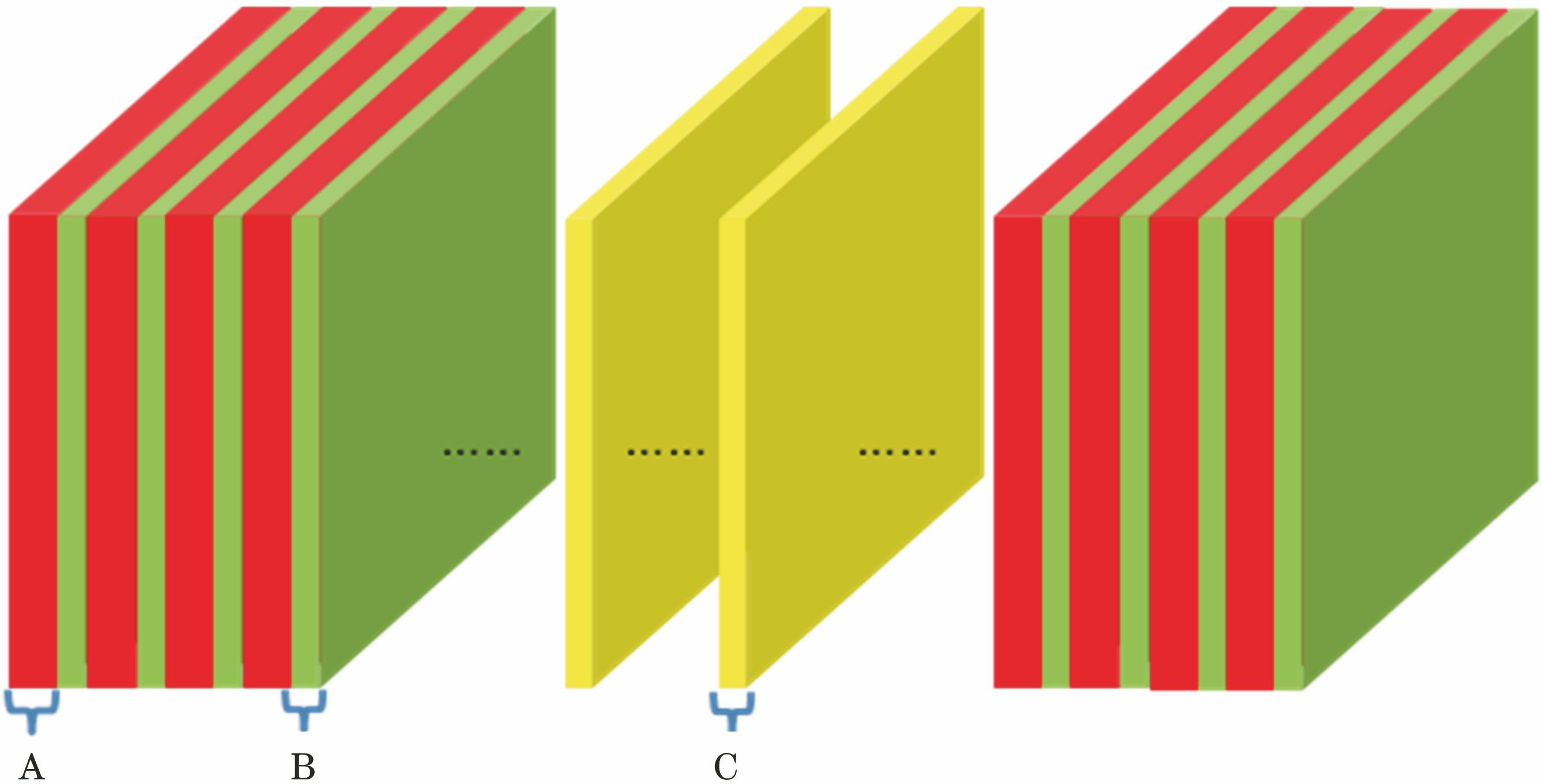
    Fig. 1. Schematic of one-dimensional asymmetric photonic crystal structure
    Defect mode position versus optical power density of 532 nm laser
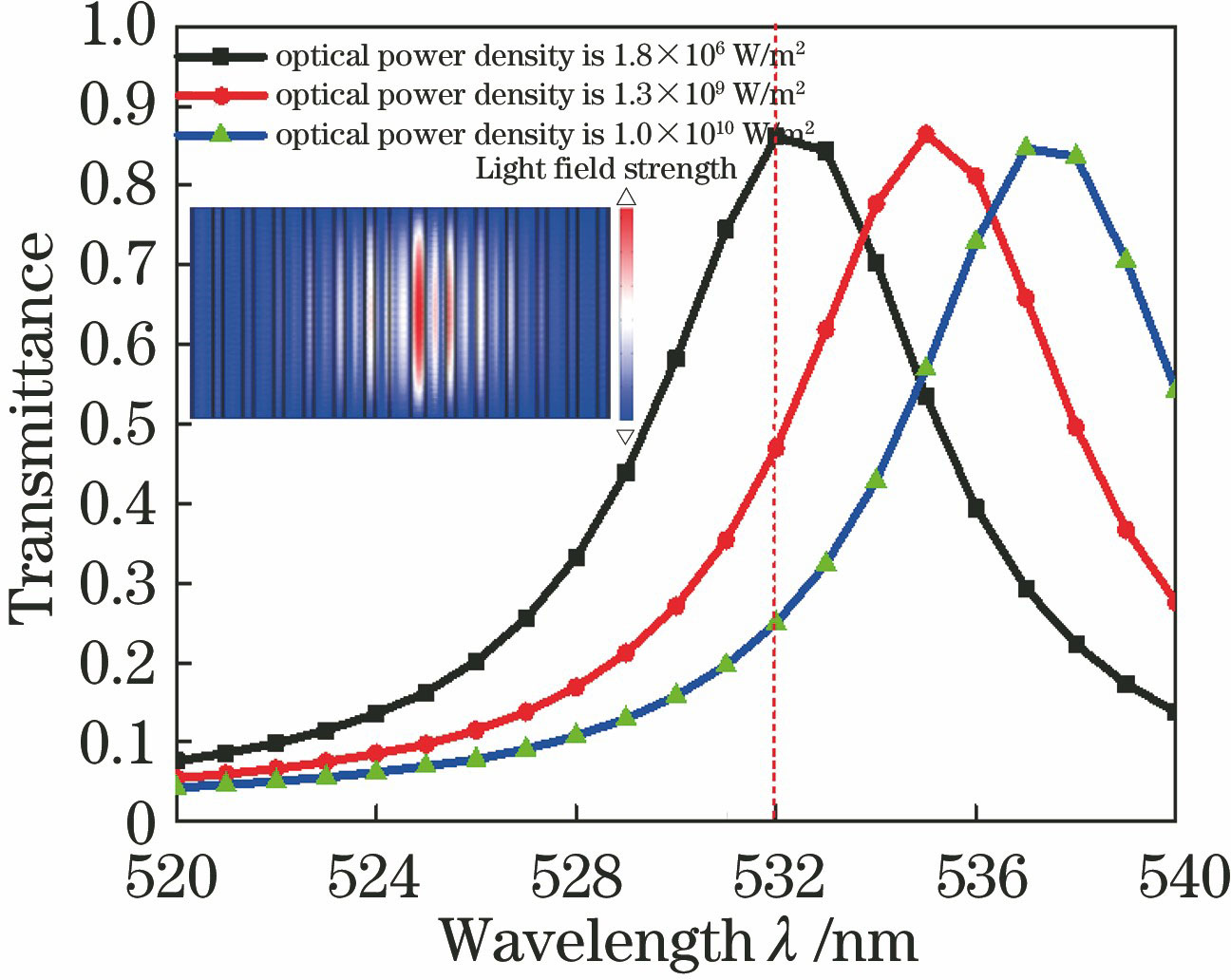
    Fig. 2. Defect mode position versus optical power density of 532 nm laser
    Defect mode position versus optical power density of 1064 nm laser
    Fig. 3. Defect mode position versus optical power density of 1064 nm laser
    Relationship between optical transmittance of 532 nm laser and optical power density of incident laser for each structure
    Fig. 4. Relationship between optical transmittance of 532 nm laser and optical power density of incident laser for each structure
    Relationship between optical transmittance of 1064 nm laser and optical power density of incident laser for each structure
    Fig. 5. Relationship between optical transmittance of 1064 nm laser and optical power density of incident laser for each structure
    Effects of thickness fluctuations (within ±5.0 nm) of other two dielectric layers on peak transmittance when thickness of one dielectric layer is constant. (a)Thickness of dielectric layer A is 184.1 nm; (b) thickness of dielectric layer B is 92.0 nm; (c) thickness of dielectric layer C is 138.1 nm
    Fig. 6. Effects of thickness fluctuations (within ±5.0 nm) of other two dielectric layers on peak transmittance when thickness of one dielectric layer is constant. (a)Thickness of dielectric layer A is 184.1 nm; (b) thickness of dielectric layer B is 92.0 nm; (c) thickness of dielectric layer C is 138.1 nm
    Effects of thickness fluctuations (within ±5.0 nm) of other two dielectric layers on peak transmittance when thickness of one dielectric layer is constant. (a) Thickness of dielectric layer A is 149.3 nm; (b) thickness of dielectric layer B is 74.7 nm; (c) thickness of dielectric layer C is 112.0 nm
    Fig. 7. Effects of thickness fluctuations (within ±5.0 nm) of other two dielectric layers on peak transmittance when thickness of one dielectric layer is constant. (a) Thickness of dielectric layer A is 149.3 nm; (b) thickness of dielectric layer B is 74.7 nm; (c) thickness of dielectric layer C is 112.0 nm
    LayerThickness-determined dielectric layer
    ABC
    Range of variablethickness /nm±0.5±0.5±0.5
    Table 1. Statistical results of transmittance varying with dielectric layer thickness
    LayerThickness-determined dielectric layer
    ABC
    Range of variablethickness /nm±2.0±1.5±1.5
    Table 2. Statistical results of transmittance varying with dielectric layer thickness
    Jialing Shen, Yuangang Lu, Haixia Ma, Jiming Wang, Feng Xu, Dunwen Zuo. Nonlinear Laser-Limiting Method Based on One-Dimensional Photonic Crystals with Double Defects[J]. Chinese Journal of Lasers, 2019, 46(8): 0808001
    Download Citation