Abstract
Based on the hybrid integration technology, an ultra-compact and low cost transmitter optical subassembly module is proposed. Four directly modulated lasers are combined with a coarse wavelength division multiplexer operated at the O-band. The bandwidth for all channels is measured to be approximately 3 GHz. The transmission is experimentally demonstrated for a 10 km standard single mode fiber (SSMF), in which an optical isolator is used for avoiding the back-reflected and scattered light to improve the bit error rate (BER) performance. A low BER and clear eye opening are achieved for 10 km transmission.The rapid growth of internet traffic provokes an urgent and strong demand on network capacity. Currently, the optical network is already extensively employed and commercialized in a data center[1,2]. Since 2010, Institute of Electrical and Electronics Engineers (IEEE) has standardized 100 GBASE-LR4 for 10 km reach application[3,4]. In this scheme, four directly modulated lasers (DMLs) are adopted due to their advantages in low power consumption. The DMLs are operated at near 1310 nm with wavelength spacing of 4.5 nm, which corresponds to the local area network wavelength division multiplexer (LAN-WDM) grid. However, due to the rigorous wavelength accuracy between the DMLs and the LAN-WDM, a thermo-electric cooler (TEC) has to be required to maintain a stable operation environment. There is no doubt that this will increase power consumption. Therefore, in order to further lower the power consumption, 100G coarse wavelength division multiplexer (CWDM4) technical specifications were standardized by the multi-source agreement (MSA) group for the 2 km reach application in 2014. Furthermore, 100G-4WDM-10 technical specifications were also defined to meet the demand of 10 km transmission in 2017[5]. The wavelength spacing between DMLs has increased to 20 nm, which corresponds to the CWDM. Enough wavelength spacing enables the DMLs to operate without cooling, which helps to save on costs.
Generally, there are two schemes for the integration of four DML chips. One is the monolithic integration, in which four chips are fabricated on a shared wafer[6–8]. Although the size of the monolithically integrated DML array chip can be minimalized, it requires a sophisticated technology regarding the wavelength control, electrical isolation between chips, etc. Moreover, any defect of any one channel will lead to the unavailability of the whole chip. Therefore, the cost will be increased. The other is the hybrid integration, in which four discrete chips are mounted on a shared carrier[9–12]. This scheme has advantages of being simple, optional, and with low cost. Therefore, it is often adopted in the optical network configuration of , , or even a larger capacity.
In this Letter, we develop an ultra-compact and cost-effective transmitter optical subassembly (TOSA) module. The operation wavelengths are 1269.5, 1289.7, 1309.6, and 1329.7 nm, which will coincide with the CWDM grid. Employing the hybrid integration technology, four DML chips are accurately mounted on a shared carrier with a pitch of 0.75 mm. Four focusing lenses are used between the DMLs and the silicon-based CWDM to realize a high coupling efficiency. The size of the package body is only . Using the module, we experimentally demonstrate the on-off keying (OOK) signal transmission for a 10 km standard single mode fiber (SSMF) with each channel modulated at . In order to avoid the back-reflected and scattered light in the SSMF transmission, an optical isolator (OI) is used. The improved bit error rate (BER) performance and the eye diagrams are observed for various cases. Furthermore, a four level pulse amplitude modulation (PAM-4) transmission is also performed.
Sign up for Chinese Optics Letters TOC. Get the latest issue of Chinese Optics Letters delivered right to you!Sign up now
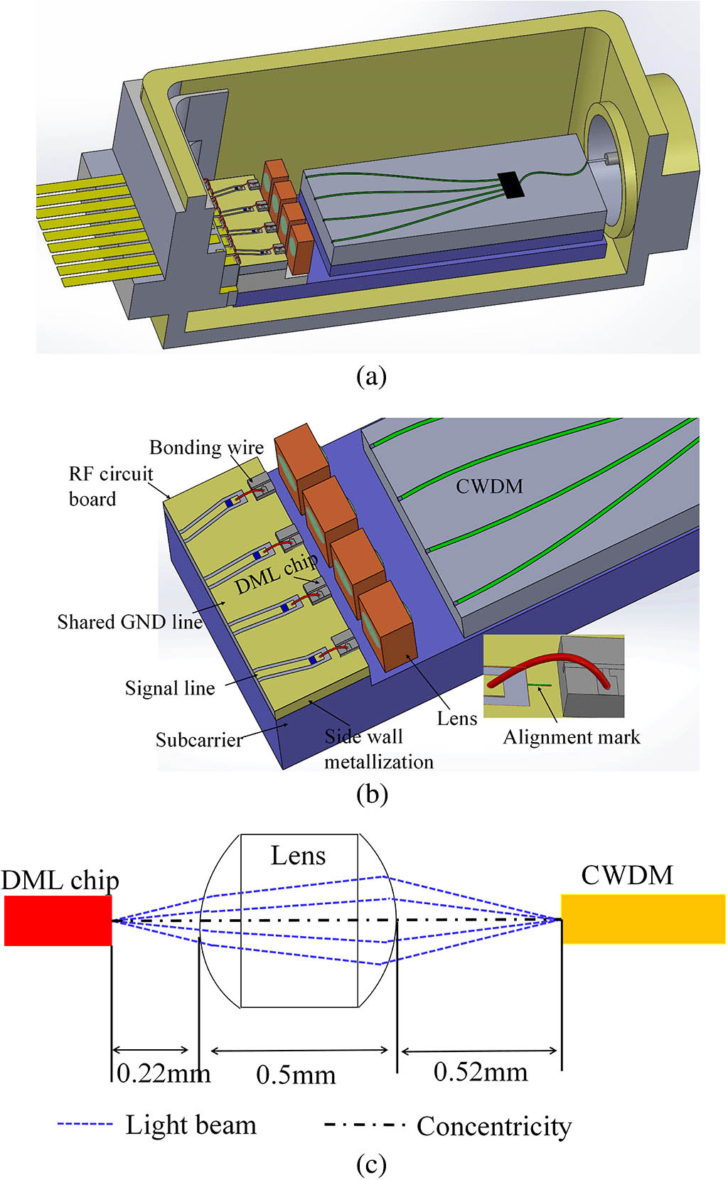
Figure 1(a) shows the proposed TOSA module configuration. In consideration of low fabrication complexity and a highly configurable feature, hybrid integration technology is selected as the optimal solution for the compact TOSA module. In the module, it consists of a ultra-compact package body, a radio frequency (RF) circuit board, four DML chips, four focusing lenses, a silica-based CWDM operated at the O-band with 20 nm wavelength spacing[13], and some subcarriers to support various elements. The partially detailed configuration is shown in Fig. 1(b). It can be seen that on the surface of the RF circuit board, four grounded coplanar waveguide (GCPW) transmission lines are fabricated. The electrode of the DML chip is placed on the RF circuit board by soldering and then connected to the shared ground line. Meanwhile, the electrode is connected to the signal line by bonding wire. The RF circuit board, four focusing lenses, and the multiplexer are fixed on a subcarrier. The pitch of chips, as well as the lenses, is 0.75 mm, which is consistent with that of multiplexer channels. Considering a high accuracy is required on the chip placement using hybrid integration technology, the alignment mark is fabricated on the RF circuit board, which can ensure the minimum alignment error, as the inset shown in Fig. 1(b).

Figure 1.(a) Hybrid integrated CWDM TOSA module configuration. (b) Schematic structure of DML array subassembly. Insertion shows the alignment mark. (c) Optical coupling configuration.
For an optoelectronics device, optical coupling is critical to maintain the stable optical output power. Generally, in the hybrid integrated TOSA module, the direct coupling between the chip and the multiplexer is considered as an effective and simple solution. However, due to the divergence characteristic of the laser’s output beam, the coupling efficiency is rather low using the direct coupling method. Therefore, four focusing lenses are used to focus the divergent light of the laser into the multiplexer. Figure 1(c) shows the optical coupling scheme in the proposed TOSA module. It is worth noting that in order to achieve high optical coupling efficiency, the height of the output waveguide of the chip, the center optical axis of the lenses, and the input waveguide of the multiplexer should be carefully adjusted to keep a low concentricity error. Furthermore, the distances between the chip and lenses and between the lenses and multiplexer are optimized to 0.218 and 0.518 mm, respectively. The distance between the chip and the multiplexer is 1.236 mm with a 0.5 mm lens thickness. After optimization, the coupling efficiency can be more than 80%. Finally, a Lucent Connector receptacle is directly attached to the edge of the output waveguide of the multiplexer.
Figure 2 shows the proposed model of the RF circuit board, on which the high frequency GCPW transmission lines are fabricated. The RF circuit board is made of AlN ceramic. The length is 3 mm. The width is 1.25 mm, and the thickness is 0.25 mm. The intrinsic resistance of the DML chip we used is about 10 Ω, thus a 40 Ω matching resistor is used and placed in series with the chip in order to match with the 50 Ω measurement system. The width of the signal line is 0.09 mm. The gap between the signal line and ground line is 0.04 mm. The ratio of the width and the gap determines the characteristic impedance of the transmission line. In the conventional GCPW transmission line, ground lines are isolated, which will introduce the electrical crosstalk. It is preferable to use a via hole to get a good ground connection between the top surface and the rear surface of the RF circuit board. However, the diameter and the pitch of via holes require a careful design otherwise the transmission performance will be greatly influenced. Moreover, the fabrication of via holes is also complicated, which can increase the cost. In order to simplify the process and save on cost, we propose a simple and effective method to achieve the ground connection between all ground lines, as described in Fig. 2. The side wall metallization is used to connect the ground line between the top surface and the rear surface of the RF circuit board instead of via holes. Therefore, the improved physical shielding is achieved, which will help to decrease the electrical crosstalk.
Figure 2.Model of RF circuit board with high frequency GCPW transmission line.
Figure 3 shows the measured transmission response for all lanes. It can be seen that the insertion loss is about 1.7, 1.3, 1.3, and 1.5 dB up to 30 GHz for lanes 1, 2, 3, and 4, respectively. Before measurement, the test system has been calibrated for eliminating the effect of the probe and cable. We can see from the measured result that due to the matching resistor, the signal power has about 2.5 dB loss at a low frequency. Furthermore, the introduction of shared ground brings lower electrical crosstalk, as the inset of Fig. 3 shows. The electrical crosstalk can be suppressed below in a range from the DC to 30 GHz.
Figure 3.Measured transmission response of the RF circuit board. Inset exhibits the electrical crosstalk between adjacent lanes.
The frequency response of the package body is measured, as shown in Fig. 4. It can be seen that the insertion loss of all four lanes is within 3 dB at 30 GHz. The reflection is maintained below at 17 GHz and at 30 GHz. These measured performances enable the RF circuit board and the package body to support the signal transmission.
Figure 4.Measured transmission response and reflection response of the package body.
Figure 5 shows the measured transmission response of the packaged TOSA module. It can be seen that for all lanes, the 3 dB bandwidth is about 3 GHz at a 30 mA current. Meanwhile, the 10 dB bandwidth can approximately reach up to 18.2, 17.8, 17.2, and 16 GHz for lanes 1, 2, 3, and 4, respectively. That is sufficient to support up to signal modulation. For a higher modulation speed, some bandwidth enhancement methods are inevitably required for compensating for the limited device bandwidth, such as the pre-compensation method. The complexity of the pre-compensation method is thought to depend, in a way, on the bandwidth characteristic of the device. As exhibited in Fig. 5, the transmission response curve of the proposed module is slowly dropped. Therefore, the reduced response can be more easily improved using the pre-compensation method compared to the case in which the response is rapidly dropped at high frequency. The packaged TOSA module has a compact size, as the inset of Fig. 5 shows. The size is only . The inner distribution is also observed in detail.
Figure 5.Measured transmission response of the packaged TOSA module. Inset is the photograph of the module with a size of , and the detailed inner distribution is also shown.
Figure 6 shows the measured power-current (P-I) characteristics of the TOSA module. With the help of the hybrid integration scheme, the output power of lanes 1 to 4 is larger than 2.5 mW with the injection current of 40 mA in spite of the approximately 6 dB coupling loss between the chip and the single mode fiber pigtail, which can meet the demand of the 10 km SSMF transmission. The inset of Fig. 6 exhibits the measured optical spectrum characteristics. It can be seen that the wavelengths of lanes 1 to 4 are 1269.5, 1289.7, 1309.6, and 1329.7 nm, respectively, which coincide with the CWDM grid as the colored areas indicate. The channel spacing is about 20 nm, which has a good agreement with the channel spacing of the multiplexer. The side-mode suppression ratios (SMSRs) exceed 40 dB for all lanes, and the TOSA exhibits clear single mode operation. These SMSRs meet the 100G-4WDM-10 specification ().
Figure 6.Measured P-I characteristics of the TOSA module. Inset is the lasing optical spectrum (colored areas indicate CWDM grid).
In order to verify the high speed transmission performance of the proposed TOSA module, we perform a transmission experiment for the 10 km SSMF. Figure 7 shows the measurement setup. A pseudorandom binary sequence (PRBS) signal is generated using a bit pattern generator (BPG). Due to the limited signal amplitude, an EA with 3 dB bandwidth of up to 38 GHz has to be used to amplify the BPG output. To achieve a uniform output power for all lanes, the bias current of lane 2 to lane 4 is set at 35 mA, and that of lane 1 is set at 30 mA, providing an output power of approximately 2.5 mW. After back-to-back (BTB) and 10 km transmission, the modulated optical signal is received and converted to the RF signal by a high speed photodetector (PD) with 18 GHz bandwidth integrated with a transimpedance amplifier (TIA). For the 10 km case, an OI has to be used to prevent the reflected light back to the chip. Before the PD, a VOA is employed to adjust the received optical power (ROP). The received RF signal is finally recorded by a real-time digital sampling oscilloscope (DSO) with an analog bandwidth of 33 GHz and processed off-line.
Figure 7.Experimental setup for the 112 Gb/s 10 km transmission system with direct detection. BPG, bit pattern generator; EA, electrical amplifier; OI, optical isolator; VOA, variable optical attenuator; PD, photodetector; TIA, transimpedance amplifer; DSO, digital sampling oscilloscope.
Figure 8 shows the measured BER characteristics versus ROP under operation. It can be seen that for the BTB case, a good BER performance is achieved, and the clear eye opening (III) is achieved with a BER of . The receiver sensitivity of lanes 1 to 4 at the forward error correction (FEC) limit of is about , , , and , respectively. However, for a BER of about , the corresponding eye diagram shows relatively large intensity noise (IV). In optical fiber transmission, it can excite the back-reflected and scattered light, which can strongly affect the performance of the modulated signal. Therefore, for the 10 km SSMF transmission case, an OI has to be used to prevent the deterioration effect of reflected light on transmission performance. As observed in Fig. 8, without an OI we cannot achieve a BER lower than the FEC limit of , and the corresponding eye diagram (I) is severely closed. Here, we only choose lane 1 for the comparison. With OI, the BER performance is greatly improved. A clearly opened eye diagram (II) is observed at a BER of . The BER performance is different after the 10 km SSMF transmission due to the chirp of the DML and the dispersion of the fiber[14–16]. The receiver sensitivity at the FEC limit is about , , , and for lanes 1 to 4, respectively.
Figure 8.Measured BER characteristics versus the ROP under operation for BTB 10 km with OI, 10 km without OI cases. Insets exhibit the eye diagram characteristics for various cases.
We further study the PAM-4 signal transmission performance using the fabricated TOSA module. To simplify the analysis, we still only choose lane 1 to be measured. Figure 9 demonstrates the comparison of PAM-4 and the OOK signals at . Here, the signal length is set to for comparison purposes. The receiver sensitivity of the PAM-4 signal for the BTB case is measured to , which is 3.3 dB worse than the sensitivity of the OOK signal. This is because the PAM-4 signal suffers the limited linearity of the DML. After 10 km transmission over the SSMF, there is a power penalty of approximately 1 dB. The eye diagrams for various cases can be clearly observed. Therefore, we can infer that the proposed TOSA module can support the minimum PAM-4 signal transmission for the 10 km SSMF.
Figure 9.Measured BER as a function of ROP for various cases under PAM-4 and OOK operations. Insets show the eye diagram characteristics.
In conclusion, an ultra-compact TOSA module is demonstrated. Based on the hybrid integration technology, four discrete DML chips are integrated into an ultra-compact package body together with a CWDM operated at the O-band. In order to increase the optical coupling efficiency, four lenses are used to focus the light into the multiplexer. The fabricated TOSA module is only in size for a C form-factor pluggable (CFP2) or smaller 100 GbE transmitter. For all lanes, the measured bandwidths are 3 GHz. The transmission for the 10 km SSMF is performed. The results show that a receiver sensitivity of up to is obtained for the BTB case. After 10 km transmission, the receiver sensitivity is , , , and for lanes 1 to 4, respectively. Furthermore, the PAM-4 transmission performance is also measured. These results indicate that the proposed TOSA module provides a low cost and effective candidate for a 100 GbE optical network or larger capacity.
References
[1] X. Zhou, H. Liu, R. Urata. Chin. Opt. Lett., 15, 120008(2017).
[2] Y. Li, Y. Zhang, L. Zhang, A. W. Poon. Photon. Res., 3, B10(2015).
[3] 3
[4] M. Kawamura, F. Nakajima, H. Oomori, H. Hara, A. Yasaki. Infocommunications, 80, 66.
[5] 5
[6] S. Kanazawa, W. Kobayashi, Y. Ueda, T. Fujisawa, T. Ohno, T. Yoshimatsu, H. Ishii, H. Sanjoh. Opt. Express, 24, 13555(2016).
[7] S. Kanazawa, W. Kobayashi, Y. Ueda, T. Fujisawa, K. Takahata, T. Ohno, T. Yoshimatsu, H. Ishii, H. Sanjoh. J. Lightwave Technol., 34, 3646(2016).
[8] G. Li, D. Lambert, J. Zyskind, J. Spann, M. Askari, G. Pickrell, M. Sodagar, S. Krasulick. International Conference on Group IV Photonics (GFP), 164(2016).
[9] H. Y. Kao, Z. X. Su, H. S. Shih, Y. C. Chi, C. T. Tsai, H. C. Kuo, C. H. Wu, J. J. Jou, T. T. Shih, G. R. Lin. J. Lightwave Technol., 36, 703(2018).
[10] J.-S. Huang, X. He, H. Blauvelt, H. Chin, M. Lomeli, R. Zendejaz, C. Lei. IEEE Photonics Conference, 461(2015).
[11] T. Nakajima, T. Fukamachi, M. Akashi, A. Nakamura, Y. Sakuma, S. Hayakawa, R. Washino, M. Mukaikubo, K. Okamoto, K. Motoda, K. Naoe, K. Nakahara, S. Tanaka, K. Uomi. Optical Fiber Communications Conference and Exhibition, 1(2015).
[12] Z. Zhao, Y. Liu, Z. Zhang, X. Chen, J. Liu, N. Zhu. Chin. Opt. Lett., 14, 120603(2016).
[13] J.-M. An, J.-S. Zhang, L.-L. Wang, K. Zhu, B. Sun, Y. Li, J. Hou, J.-G. Li, Y.-D. Wu, Y. Wang, X.-J. Yin. Opt. Eng., 57, 1(2018).
[14] T. Tadokoro, W. Kobayashi, T. Fujisawa, T. Yamanaka, F. Kano. J. Lightwave Technol., 30, 2520(2012).
[15] W. Kobayashi, T. Fujisawa, K. Tsuzuki, Y. Ohiso, T. Ito, S. Kanazawa, T. Yamanaka, H. Sanjoh. J. Lightwave Technol., 32, 3(2014).
[16] T. Ito, O. Slezak, M. Yoshita, H. Akiyama, Y. Kobayashi. Photon. Res., 4, 13(2016).