Abstract
The research on high power 110 GHz single and power-combined frequency doublers based on discrete diodes is presented in this paper. The doubler with a single Schottky diode circuit has a measured peak efficiency of 33% and bandwidth over 13.6%. Meanwhile, two different architectures with two single devices adding in-phase have been utilized to realize the power-combined doublers. The combined doubler features four discrete Schottky diodes with twelve junctions altogether soldered on two 127 μm-thick ALN substrates. Both devices have demonstrated output powers more than 200 mW with a pumping power over 800 mW and are capable of providing more power for higher driven power.Introduction
Over the years,multipliers based on Schottky diodes operating in the 100~115 GHz range are in demand for variety of applications. These devices play a critical role in system such as terahertz communications[1]and millimeter and submillimeter-wave radars or radiometers[2],which hold great potential in security applications such as mass transit security,surveillance and person-borne concealed weapons detection. Providing as high powers as possible is critical for terahertz communications and radars to operate at long range or multiple pixel arrays which would distribute signal power to several transmitters and receivers[3]. Mostly,the operating frequencies of these applications are preferred to locate around 220,330,and 670 GHz,within the atmospheric absorption windows.
Generally,the generation of powers at frequencies up to 670 GHz typically requires several stages of multiplication and amplification,which completely depends on sufficient powers over 100~115 GHz range. However,there are no commercial amplifiers available for sale,to the author’s knowledge,which extend beyond 110 GHz with output power over 100 mW. Thus,Schottky based frequency sources are the most preferred technology to generate relative high power in terahertz ranges. Serving as the driven stage in a THz frequency multiplier chain,doublers working in 100~115 GHz range should have high conversion efficiency,enough bandwidth and sufficient power capacity. However,the output power of the traditional single balanced doubler is limited due to the power capacity of Schottky diodes. And the solution incorporates the in-phase combination of several diode circuits[4],which helps these devices to handle on much higher power.
In this paper,we have developed the broadband high-performance single and power combined frequency doubler based on the balanced configuration in Ref.[5]. The proposed single doubler is developed based on our previous work in Ref.[6],by optimizing the diode models,developing the solder pre-coat technology and make use of the equivalent symmetric conditions. Meanwhile,two kinds of power-combined doublers are developed with different in-phase combination configurations,both of which are demonstrated to provide an output power over 200 mW with pumping power over 800 mW.
1 Single doubler
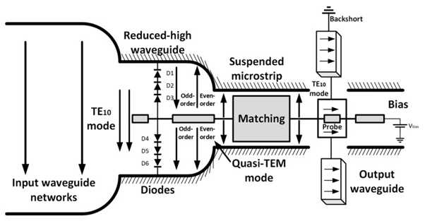
The applied doubler configuration in this paper is the so-called Erickson-style structure[7],which relies on the inherent mode and frequency isolation between the input and output ports. The core element is a pair of discrete diodes placed in anti-series configuration at the junction between the balanced and unbalanced sections of the circuit. Figure 1 illustrates architecture of the doubler circuit discussed in this work. The incident signal operating in TE10 mode is coupled to the varactors and is cut off by the suspended circuit channel,which could be realized through narrowing down the channel width. Meanwhile,a reduced-height input waveguide is needed to prevent the field distribution called TM11 mode of the second harmonic.

Figure 1.Diagram of the doubler circuit architecture.
Our previous work in Ref.[6]showed a peak output power of 108 mW@109 GHz(Pin=28 dBm)with undesired great spectrum ripples and ultra-low efficiency,which were caused by the over-estimated parasitic capacitor values as well as the performance degradation introduced by the thermal effect under high power condition in diode junctions. In this work,the value of parasitic capacitor has been calibrated from 4 fF to 1.4 fF according to our previous research. Also the circuits design makes use of equivalent boundary condition to analyze the fundamental and second harmonic signals individually,which is the key methodology to make progress in improving the conversion efficiency. Further details of the design methodology have been discussed in Ref.[7]. Besides,the solder pre-coat technology was developed to replace the traditional silver conductive paste,which could provide much better stability and lower parasitic loss. Moreover,ALN ceramic substrates with high thermal conductivity have been utilized to provide a better heat sink path.
Determining embedding impedance of each junction at the internal coaxial wave port should be the first step to design the proposed doubler. Meanwhile,dimension of the adopted diode is 248 m*50 m*10 m,which is comparable with the wavelength at 110 GHz. As a result,evaluation of the optimum embedding impedance must consider the influence of the diode on field distribution. A co-simulation of the diode is carried out by HFSS and ADS to determine the optimum embedding impedance at each diode junction. The extracted results from full-wave simulation take part in the calculation of optimum impedance with the nonlinear model of varactors. Finally,the determined diode optimum impedance to incident frequency Zin(f0)is 13.2-j*76.7,while to output second harmonic Zout(2f0)is 18.5-j*38.3. According to that,the balanced 110GHz doubler in Fig. 2 has been synthesized,which is composed of two discrete diodes,a 127 um thick ALN substrate(2.865*0.84*0.127 mm)and waveguide impedance matching networks. The circuit parameters and dc reverse bias voltage were carefully optimized to maximize the efficiency for an input power of 300~400 mW.
Figure 2.(a) Field distribution of incident frequency, and (b) field distribution of output second harmonic in the proposed doubler
The width of the reduced-height waveguide and suspended channel is 0.74 mm and 0.64 mm respectively,with 0.88 mm wide slot to place the 0.84 mm wide substrate. The selected waveguide width can effectively suppress the high order TM11 field distribution(fcTM11=206.6 GHz),which is similar to the output second TEM mode harmonic. The broadband performance is achieved with a series of waveguide sections to provide wide band impedance matching to the diodes. Figure 2(a)shows the fundamental wave distribution in the whole doubler network,which is cut off by the suspended circuit channel because of the mode isolation. Similarly,field distribution in Fig. 2(b)indicates that the generated second harmonic waves could not exist in the input waveguide networks because the successful harmonic isolation design.
Figure 3(a)shows a 3D view of the proposed doubler in half of the split block. The whole E-plane split-waveguide block with a volume of 20 mm×20 mm×15 mm is fabricated by computer numerical control milling technology. Then,the utilized discrete diodes are carefully mounted on the ceramic circuit with preformed solder. The planar circuit is assembled above the split block by silver conductive paste and the DC-bias connection is carried out through bonding to the glass-insulator. The ALN ceramic substrates,which hold advantages of high thermal conductivity and low tangent loss angle(0.001),are chosen to construct the whole planar circuits. The high thermal conductivity of ALN substrates provides a perfect heat sink path for varactors,which prevent the junctions from thermal breakdown and improve the power handling capacity. Besides,the solder pre-coat technology also has been analyzed to improve the performance stability as well as reduce the parasitic loss. The assembly picture using solder per-coat technology is illustrated in Fig. 3(b).
Figure 3.(a) Photograph of the fabricated D-band doubler, and (b) picture of the mounted 127 m-thick ALN doubler circuit
2 Power-combined doublers
The power combining configurations proposed in Ref.[8]and Ref.[9]were utilized to design two kinds of 100~115 GHz doublers in this paper to increase power capacity by a factor of two. Figure 4(a)and(b)show the basic architecture of these two kinds of power combined 100~115 GHz doublers,respectively. By using a 3dB quadrature hybrid,circuit in Fig. 4(a)has the advantage of high RF isolation and short electrical length at output,which reduce the impedance traction between two single doubler channels and help to achieve a great performance. On the other hand,doubler in Fig. 4(b)utilizes a pair of T-junction,resulting in compact structure except a longer electrical length at output.
As shown in Fig. 4(a),the input stage of doubler A is composed of a pair of balanced doublers discussed in section 1,which are driven by a 3 dB quadrature hybrid. This topology results in two inputs at the fundamental input frequency(f0)with a phase difference of ±90 degree. As a result,signals at two output ports at the 2nd harmonic(2f0)would be out of phase and the power could be combined effectively simply with a T-junction waveguide power combiner. There are three networks comprising the circuit:1)a stepped waveguide(WR15)impedance matching networks;2)two balanced planar doublers optimized to provide proper source impedance to the input port at f0 and load impedance to the output port at 2f0;and 3)An E-plane T-junction networks to achieve the power combination at 2f0 implemented in WR8 waveguide. An E-plane split-waveguide block with a volume of 20 mm×20 mm×45 mm is fabricated by computer numerical control milling technology with gold-plated. And two planar circuits are assembled above the split block using solder per-coat technology and each DC-bias connection is carried out through bonding to a glass-insulator.
Another design concept of doubler B is displayed in Fig. 4(b),which makes the use of a pair of T-junction waveguide power combiner to realize the combination with higher volumetric efficiency. The input stage of doubler B also contains a pair of balanced doublers discussed in section 1,which are driven by an E-plane waveguide T-junction rather than a 3dB quadrature hybrid. So,the input signal would be divided into two equal parts that are out of phase at the fundamental frequency. As a result,the outputs of each path would be in-phase with the frequency doubling. Thus,an in-phase combination based of a waveguide T-junction layout has been carefully designed to complete the power synthesis. It is worth to note that special attention should be paid to the directions of the two output waveguides as well as keeping the balance of the two arms of the T-junction combiner. In this way,a high combining efficiency could be achieved with good in-phase characteristic. The whole circuit are fabricated in an E-plane split-waveguide block with a volume of 24 mm×19 mm×29 mm,only half the volume of circuit A. There are also two separated glass insulators to provide DC-bias two each pair of diodes.
Figure 4.(a) Photograph of the D-band power-combined doubler A, (b) Photograph of the D-band power-combined doubler B
3 Results and Discussion
3.1 Single Doubler Measurement
Characterization of the doubler is done using the experimental setup shown in Fig. 5. The input 16.67~19.2 GHz signals are supplied by an Agilent E8257D frequency synthesizer,while the output power of this D band doubler is measured by the Erickson PM5 power meter at room temperature. Measurement of the doubler was finished at the Microsystem and Terahertz research center.
Figure 5.Test configuration of the proposed D band doubler
During the test,a 50~58 GHz medium power driver chain is utilized for the pumping power over 25 dBm. As shown in Fig. 6(a),the input power of the 100~115 GHz doubler is basically larger than 280 mW in the band of 100~115 GHz except some points with output power lower than 250 mW.
Figure 6.(a) Test results of the pumping power of D band doubler. (b) Measured results of the output power of the single D band doubler
To place the varactors in reverse bias,a voltage with positive polarity through the DC bias channel is required because of the diodes’ orientation. The measured output powers and conversion efficiency driven by 250~390 mW input power from 50 to 57.5 GHz are presented in Fig. 6(b). During the measurement,the DC-bias voltage is optimized to obtain the best performance in the band of 99.9~115.2 GHz. As shown in Fig. 5(b),a peak output power of 96.54 mW is achieved at 104.6GHz with an optimized bias voltage,while the peak conversion efficiency is 33.26% at 103.2 GHz. And a high output power over 70 mW in the band of 102~112 GHz has been obtained on condition that the positive bias voltage is adjusted to 12 V. Over the operating frequency band,there is a slight difference between the measured and simulated output power,which changes from 1.02 to 1.89 dB with different frequencies. The decrease in output power could be introduced by the drift of series impedance and junction capacitance of the diodes with temperature increase caused by high operation power. Moreover,the assembly errors of circuit might make the imbalance among junctions greater which directly decrease the output power and efficiency too.
3.2 Power Combined Doubler Measurement
Measurement of the doubler is also completed using the same experimental setup shown in Fig. 5. The only difference is the doubled driven power over 800 mW in 50~58 GHz range. As shown in Fig. 7(a),the input power of the 100~115 GHz doubler is basically over 500 mW in the band of 100~115 GHz with a peak power near 950 mW. Also,varactors of the power-combined doubler are negatively biased through two insulators.
The measured output power and conversion efficiency is presented in Fig. 7(b). And the DC-bias voltage is adjusted to +12 V to obtain the best output power in the band of 100~115 GHz. As shown in Fig. 7(b),a peak output power of 211.4 mW is achieved at 102.2 GHz,while the peak conversion efficiency is 29.6% at 102.5 GHz. And the typical value of the output power over 100~115 GHz is proved to be 110 mW,with a 3 dB bandwidth of 13.6%. It can be seen that the power and efficiency of the doubler shows a slight distortion compared to the simulated results. Meanwhile,the efficiency and output power tend to be higher at lower frequencies. The reason leading to this phenomenon could be the mismatch and transmission losses introduced by the 3 dB quadrature hybrid.
Figure 7.Measurement of the power-combined doubler: (a) available pumping power of the V-band amplifier, (b) output power and efficiency of combined doubler A with a bias voltage of +12V, (c) output power and efficiency of combined doubler B
Figure 7(c)presents the test output power and conversion efficiency of combined doubler B. With the optimized bias voltage,a peak output power of 212 mW is achieved at 108.6 GHz,while the peak conversion efficiency is 28.36% at 102 GHz. And the typical value of the output power over 101~112 GHz is proved to be 150 mW. Compared to the single one,efficiency of this combined doubler B has dropped by 6 percent. This can be attributed to the waveguide transmission losses introduced by the V-band splitter and D-band combiner topology applied to the doubler. Unlike doubler A,the output power curves of doubler B is much flatter and more consistent with the simulate results. This improvement is achieved by the carefully designed waveguide T-junction layout with perfect amplitude and phase balance. Also,there is a small discrepancy between simulated and measured results when it comes to the efficiency and output power. It is believed that dielectric losses of substrates and/or series resistance values of Schottky junctions used in simulations were overestimated. A summary of the comparison between these measured performances with the reported frequency doublers is listed in Table 1.
| Ref | Anodes | Pin(mW) | Peak power(mV) | Efficiency | Band(FBW%) | Comment |
|---|
| [4] | 4×2 | 500 | 130 mW@180 GHz | 20~37% | 170~188 GHz(10%) | H-plane combined |
| [6] | 6 | 300~600 | 108 mW@110 GHz | 10~22% | 102~114 GHz(11%) | Single |
| [9] | 4×2 | 250~400 | 40 mW@178 GHz | 10~12% | 172~196 GHz(13.3%) | E-plane combined |
| [10] | 6×2 | 800~900 | 195 mW@116 GHz | 10~30% | 100~120 GHz(17%) | E-plane combined |
| [11] | 6×2 | 300~600 | 59 mW@168 GHz | - | 164~172 GHz(>5%) | E-plane combined |
| This Work | 6 | 250~400 | 96.5 mW@104.6 GHz | 20~33.2% | 100~115 GHz(13.6%) | Single |
| 6×2 | 560~900 | 211.4 mW@102.3 GHz | 18~29.6% | 100~115 GHz(13.6%) | E-plane combined |
| 6×2 | 560~900 | 212 mW@108.6 GHz | 15~28.36% | 100~114 GHz(12.7%) | E-plane combined |
Table 1. Doubler performance comparison in adjacent band
4 Conclusions
A series of D band high power single and power-combined balanced doublers based on discrete Schottky diodes have been developed. An optimized balanced doubler was realized by calibrating the diode models and using the solder pre-coat technology,based on which two different power-combined doublers were fabricated. And the test performances have been proved to meet the driven power requirements of the Y-band multiplier sources. Even if the high-power amplifiers became available above 110 GHz in the future,our approach would still be very attractive to many applications because these devices can be pumped with low-cost high-power V-band amplifiers that are commercially available from many vendors worldwide.
References
[1] Cheng Wang, Bin Lu, Chang-Xing Lin et al. 0.34-THz Wireless Link Based on High-Order Modulation for Future Wireless Local Area Network Applications. IEEE Transactions on Terahertz Science and Technology, 4, 75-85(2014).
[2] Zhen-Mao Cui, Jing-Kun Gao, Bin Lu et al. Real time 3D imagiog system based on sparse MIMO array at 340 GHz. J.Infrared Millim.Waves, 36, 102-105(2017).
[3] K. Cooper, Robert J. Dengler, Nuria Llombart et al. THz imaging radar for standoff personnel screening. IEEE Transactions on Terahertz Science and Technology, 1, 169-182(2011).
[4] Colin Viegas, Hairui Liu, Jeff Powell et al. A 180-GHz Schottky diode frequency doubler with counter-rotated E fields to provide in-phase power-combining. IEEE Microwave and Wireless Components Letters, 28, 518-520(2018).
[5] P. Penfield, R. P. Rafuse. Varactor Applications(1962).
[6] Yaoling Tian, Yue He, Kun Huang et al. High power 110 GHz balanced Schottky diode frequency doubler. Infrared and Laser Engineering, 48, 139-144(2019).
[7] Yaoling Tian, Miao Li, Kun Huang et al. High efficiency 220GHz frequency doubler based on discrete Schottky diodes. J.Infrared Millim.Waves, 38, 409-415(2019).
[8] Naser Alijabbari, Matthew F. Bauwens, Robert M. Weikle. 160GHz Balanced Frequency Quadruplers Based on Quasi-Vertical Schottky Varactors Integrated on Micromachined Silicon. IEEE Transactions on Microwave Theory and Techniques, 4, 678-685(2014).
[9] Zhenhua Chen, Xiang Cheng, Wanzhao cui et al. A High-Power G-band Schottky Local Oscillator Chain for Submillimeter Wave Heterodyne Detection. Journal of Infrared, Millimeter and Terahertz Waves, 36, 430-444(2015).
[10] J.V Siles, Choonsup Lee, R Lin et al. A High-Power 105–120 GHz Broadband On-Chip Power-Combined Frequency Tripler. IEEE Microwave and Wireless Components Letters, 25, 157-159(2015).
[11] Jin MENG, DeHai ZHANG, ChangHong JIANG et al. Design of a 166 GHz high power source based on power-combined technology. J.Infrared Millim.Waves, 37, 608-612(2018).