• Acta Physica Sinica
  • Vol. 69, Issue 14, 148101-1 (2020)
Wen-Xun Wang2, Yan-Biao Ren1、*, Shi-Chao Zhang3, Lin-Cai Zhang1, Jing-Bo Qi1, and Xiao-Wu He4
Author Affiliations
  • 1College of Chemistry Chemical Engineering and Material Science, Zaozhuang University, Zaozhuang 277160, China
  • 2Beida Xianxing Technology Industry Co., Ltd., Beijing 102200, China
  • 3School of Materials Science and Engineering, Beihang University, Beijing 100191, China
  • 4State Key Laboratory for Superlattices and Microstructures, Institute of Semiconductors, Chinese Academy of Sciences, Beijing 100083, China
  • show less
    DOI: 10.7498/aps.69.20200454 Cite this Article
    Wen-Xun Wang, Yan-Biao Ren, Shi-Chao Zhang, Lin-Cai Zhang, Jing-Bo Qi, Xiao-Wu He. Preparation of three-dimensional graphene foam with controllable defects by closed-environment chemical vapor deposition method and composite electrode electrochemical performance[J]. Acta Physica Sinica, 2020, 69(14): 148101-1 Copy Citation Text show less
    Schematic of the synthesis process of a self-supporting 3D GF: (a)−(c) Low pressure closed CVD method uses a sealed quartz tube to grow graphene on nickel foam; (d) G/Ni foam coating with thin PMMA film; (e) etching to remove nickel foam After that, PMMA protected G/Ni foam; (f) self-supporting 3D GF after dissolving the thin PMMA layer with hot acetone.
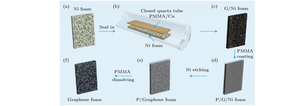
    Fig. 1. Schematic of the synthesis process of a self-supporting 3D GF: (a)−(c) Low pressure closed CVD method uses a sealed quartz tube to grow graphene on nickel foam; (d) G/Ni foam coating with thin PMMA film; (e) etching to remove nickel foam After that, PMMA protected G/Ni foam; (f) self-supporting 3D GF after dissolving the thin PMMA layer with hot acetone.
    SEM images of GF prepared with different amounts of solid carbon source: (a) 100 μL; (b) 200 μL; (c) 400 μL; (d) 800 μL.
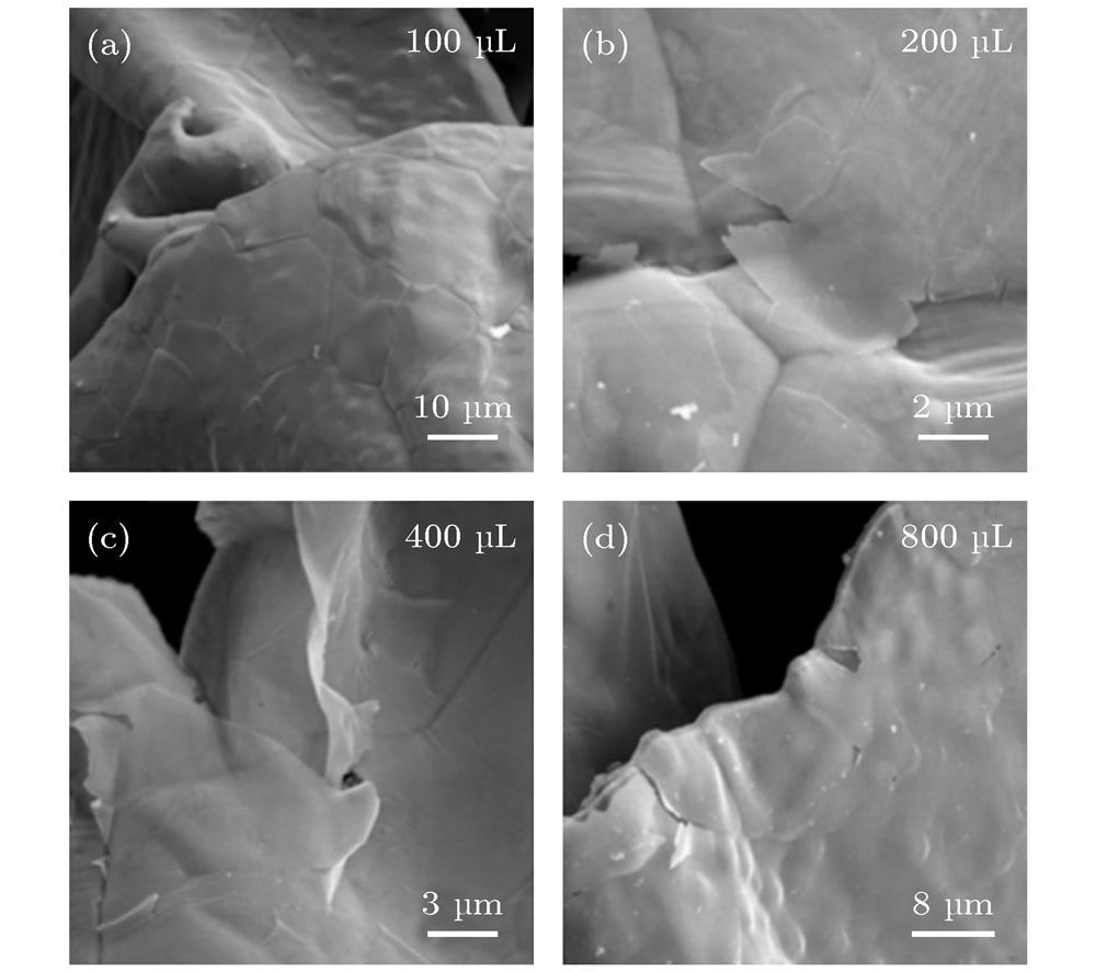
    Fig. 2. SEM images of GF prepared with different amounts of solid carbon source: (a) 100 μL; (b) 200 μL; (c) 400 μL; (d) 800 μL.
    TEM image of GF400 graphene sample prepared by low pressure closed CVD: (a) Low magnification TEM image of graphene film, showing typical wrinkle morphology; (b), (c) HRTEM image of graphene film edge; (d) electron diffraction pattern of graphene film.
    Fig. 3. TEM image of GF400 graphene sample prepared by low pressure closed CVD: (a) Low magnification TEM image of graphene film, showing typical wrinkle morphology; (b), (c) HRTEM image of graphene film edge; (d) electron diffraction pattern of graphene film.
    A graph of dispersion in the energy and frequency range for in-plane phonon modes and Raman scattering in graphene.
    Fig. 4. A graph of dispersion in the energy and frequency range for in-plane phonon modes and Raman scattering in graphene.
    SEM images of graphene foam surfaces prepared at different reaction times: (a) 2 min; (b) 5 min; (c) 10 min; (d) 20 min. (e) Raman spectra of graphene foams prepared at different reaction time.
    Fig. 5. SEM images of graphene foam surfaces prepared at different reaction times: (a) 2 min; (b) 5 min; (c) 10 min; (d) 20 min. (e) Raman spectra of graphene foams prepared at different reaction time.
    SEM images of graphene foam surfaces prepared with different hydrogen contents: (a) Vacuum; (b) 0.5 kPa; (c) 5 kPa. (d) Raman spectra of graphene foam prepared with different hydrogen contents.
    Fig. 6. SEM images of graphene foam surfaces prepared with different hydrogen contents: (a) Vacuum; (b) 0.5 kPa; (c) 5 kPa. (d) Raman spectra of graphene foam prepared with different hydrogen contents.
    SEM images of 3 D GF: (a) G/Ni foam prepared by low-pressure closed CVD method; (b) self-supporting 3D GF with low magnification; (c) self-supporting 3D GF with high magnification; (d) high-resolution TEM image of graphene sheet edge. The interlayer spacing of double-layer (2 L) and five-layer (5 L) graphene is about 0.33 nm, and the samples were prepared with 500 μL of PMMA addition.
    Fig. 7. SEM images of 3 D GF: (a) G/Ni foam prepared by low-pressure closed CVD method; (b) self-supporting 3D GF with low magnification; (c) self-supporting 3D GF with high magnification; (d) high-resolution TEM image of graphene sheet edge. The interlayer spacing of double-layer (2 L) and five-layer (5 L) graphene is about 0.33 nm, and the samples were prepared with 500 μL of PMMA addition.
    (a)−(c) FE-SEM images of ZnO/GF electrodes with different magnifications; (d) charge-discharge curves of ZnO/GF500 composite; (e) cycle curves of ZnO/GF300 and ZnO/GF500 at current densities of 0.2 A·g–1; (f) the nyqusit spectrum of ZnO/GF500 electrode after 10th and 100th cycles at a current density of 0.2 A·g–1 (inset is the equivalent circuits of ZnO/GF electrode).
    Fig. 8. (a)−(c) FE-SEM images of ZnO/GF electrodes with different magnifications; (d) charge-discharge curves of ZnO/GF500 composite; (e) cycle curves of ZnO/GF300 and ZnO/GF500 at current densities of 0.2 A·g–1; (f) the nyqusit spectrum of ZnO/GF500 electrode after 10th and 100th cycles at a current density of 0.2 A·g–1 (inset is the equivalent circuits of ZnO/GF electrode).
    圈数Rs/Ω Rf/Ω Rct/Ω CPE1/F CPE2/F
    105.615.242.36.4 × 10–56.5 × 10⁻⁴
    1004.212.421.71.9 × 10–47.8 × 10⁻⁴
    Table 1.

    Values for all the parameters of ZnO/GF500 electrode based on the equivalent circuits.

    ZnO/GF500电极基于等效电路图的各参数数值

    Wen-Xun Wang, Yan-Biao Ren, Shi-Chao Zhang, Lin-Cai Zhang, Jing-Bo Qi, Xiao-Wu He. Preparation of three-dimensional graphene foam with controllable defects by closed-environment chemical vapor deposition method and composite electrode electrochemical performance[J]. Acta Physica Sinica, 2020, 69(14): 148101-1
    Download Citation