Abstract
The diffraction of a dielectric microline pair is optimized by numerical simulations to generate an efficient focusing pattern with a micron-scale footprint. Microlines separated by 1.12 μm are fabricated by two-photon polymerization on a glass substrate, and their diffraction pattern is characterized by three-dimensional wide-field transmission microscopy. A line pair, having a width and a height , leads to diffraction-limited focusing in the visible spectrum. Depending on wavelength, its focal length, lateral resolution, and depth of focus are in the ranges of 0.8–1.3 μm, 0.22–0.44 μm, and 1.7–2.13 μm, respectively. Such a microlens based on the diffraction of only two subwavelength scatterers could be used for the design of miniature optical sensors with micron and sub-micron pixels.The miniaturization of sensors leads to a continuous trend for downsizing the pixel size. Currently, it is 1.12 μm for visible complementary metal–oxide–semiconductor (CMOS) sensors, and sub-micron sizes are under development[1]. Below 2 μm, the optical performances of refractive microlenses degrade, and alternative light collection strategies need to be investigated towards wavelength-scale pixels[2–4].
Some micron-scale plasmonics and dielectric lenses based on sub-wavelength structures have been reported[5–7]. They need at least a few periods to generate the spatial phase modulation needed for focusing. Thus, it will be difficult to downscale their sizes in the sub-micron scale.
In our previous work, we have reported on diffraction-limited microlenses with sizes in the few micron range. Efficient focusing resulted from the diffraction intensity pattern of parallel metallic nanowires[8,9]. In this work, we report on microfocusing with pairs of parallel polymer lines, separated by 1.12 μm, that do not have ohmic and reflection losses of metals. The line geometry is optimized by two-dimensional (2D) numerical simulations to obtain the focusing diffraction pattern. The experimental demonstration is done with their fabrication by two-photon polymerization (TPP) on a glass substrate and with their optical characterization by three-dimensional (3D) wide-field transmission microscopy.
Sign up for Chinese Optics Letters TOC. Get the latest issue of Chinese Optics Letters delivered right to you!Sign up now
COMSOL multiphysics (radio-frequency module) is used to execute 2D numerical simulations by the finite element method (FEM). Reflection artefacts are eliminated by perfectly matched layers. The mesh size is smaller than .
The diffraction intensity patterns are calculated for pairs of parallel dielectric lines with the rectangular section of width W and height H on a dielectric substrate with the same refractive index . Their separation distance (center to center) is set to . Calculations are done with incident plane waves with TM and TE polarizations and for monochromatic red–green–blue (RGB) colors, i.e., wavelengths of 0.60, 0.53, and 0.45 μm.
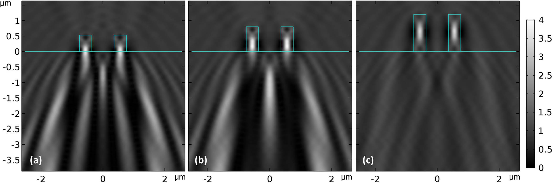
Typical diffraction intensity patterns are presented in Fig. 1. They are calculated for the TE plane wave of wavelength . The pairs of microlines have a constant width of and different heights , 0.80, and 1.20 μm. A clear microfocusing pattern is shown in Fig. 1(b) with the height . For the smaller height , the diffraction intensity pattern is complex. There is a low-efficiency focusing region with strong sidelobes, as shown in Fig. 1(a). For the larger height , the incident intensity pattern is almost unperturbed by the diffractive structures [Fig. 1(c)].

Figure 1.Diffraction intensity patterns obtained for pairs of dielectric rectangles with different heights , 0.80, 1.20 μm from left to right and width .
The phase maps of their diffraction patterns are displayed in Fig. 2. The smaller height accumulates a large phase gradient inside the rectangular structure that leads to nanojet focusing in addition to small focusing phase modulation between the lines. The larger height accumulates a rad phase delay that makes the structure cloaking for the incident plane wave. The height is optimized to generate the microfocusing pattern because it corresponds to (1) a phase delay of rad, and therefore a destructive interference below the structure that minimizes the sidelobe intensities, and (2) an efficient focusing spatial phase modulation on the total field that propagates between the structures. Thus, the microfocusing pattern of microlines is obtained only for this optimized height that leads to a delay.
Figure 2.Phase distribution obtained for pairs of dielectric rectangles with different heights , 0.80, 1.20 μm from left to right and width .
Next, the optimization of microline widths is needed to obtain the maximum focused power, i.e., the normalized intensity integrated in the focal region (). In the Mie scattering regime, the power scattered by a sub-wavelength size structure is mainly in the forward direction, and it increases with its size. In the case of microfocusing pairs with a fixed separation distance, the maximum width is limited by the minimum space that needs the incident plane wave to propagate freely between the structures. The normalized power that is focalized by structures with W ranging from 0.15 to 0.50 μm is shown in Fig. 3 (black curve). It increases with the structure width and reaches its maximum for . For larger widths, the incident wave cannot propagate freely, and the focused power reduces. As shown in Fig. 3, the optimized -dephasing height increases with W because of its effective refractive index decrease (Fig. 3 blue curve).
Figure 3.Variation of the normalized focusing power (black curve with squares) and the optimized -dephasing rectangle heights (blue curve with disks) with respect to the width.
This type of microfocusing pattern is a little sensitive to the polarization and the wavelengths, as shown in Fig. 4. The first and second rows correspond to the TE and TM polarization, respectively. The columns correspond to intensity patterns obtained for the RGB wavelengths as indicated.
Figure 4.Diffraction intensity patterns obtained for pairs of dielectric rectangles with optimized dimensions ( and ). The first and the second rows represent the TE and TM polarizations. From left to right, the columns represent the blue, green, and red wavelengths, respectively.
The microlens characteristics are summarized in Table 1. The focal lengths are in the micron range, which are comparable to the separating distance . The calculated lateral resolutions and the depths of focus are around 0.3 and 2 μm, respectively.
| Polarization | Wavelength (μm) | Zf (μm) | FWHMx (μm) | FWHMz (μm) | Imax/I0 |
|---|
| TE | Blue 0.45 | 1.3 | 0.28 | 2.13 | 3.0 |
| Green 0.53 | 1.1 | 0.27 | 2.13 | 3.3 |
| Red 0.60 | 1.0 | 0.27 | 1.90 | 3.1 |
| TM | Blue 0.45 | 1.2 | 0.25 | 1.84 | 3.6 |
| Green 0.53 | 1.0 | 0.24 | 1.70 | 3.5 |
| Red 0.60 | 0.8 | 0.30 | 1.53 | 3.1 |
Table 1. Calculated Optical Characteristicsa
Further simulations (not shown) indicate that scatterer materials with higher refractive indexes would lead to similar properties with smaller scatterer dimensions. Using substrates with higher refractive indexes would lead to higher lateral resolution with longer focal lengths and depths of focus.
In the following, we present the experimental demonstration of the microfocusing obtained with parallel polymer lines with a spacing of 1.12 μm. They are fabricated by TPP of pentaerythritol triacrylate (PETA) () on a glass cover slip using the method described in Appendix A. They have a length of 20 μm and a nominal rectangular cross-section ( and ). Cover slip borosilicate substrates with 170 μm thickness have the advantage of being easily available for high resolution microscopy with immersion objective and of mimicking the dielectric layer that is in between the microlens array and the photoactive layer in sensors.
The intensity distributions are measured by wide-field transmission microscopy using an inverted microscope (Zeiss Axiovert) with an oil immersion objective () and a Zeiss color camera Axiocam ERC 5. The experimental set-up is shown in Fig. 5. The non-polarized white light is filtered by a narrow diaphragm () to increase its spatial coherence. A piezo scanner is used to obtain stacks of RGB images with spacing of 0.40 μm. The 3D intensity distributions are reconstructed with ImageJ software[10].
Figure 5.Schematic of the experimental characterization set-up.
The 3D diffraction pattern of microlines separated by 1.12 μm is shown in Fig. 6. The light is propagating along the axis. On the color 3D view [Fig. 6(a)], one can clearly distinguish the parallel lines that correspond to the light getting out of the polymer lines at and a white spot at around that corresponds to the microfocusing region. The 3D intensity distributions for RGB colors are shown in Fig. 6(b). They are similar to the calculated distributions in Fig. 4. In difference, they have less contrast due to the limited resolution of the microscope objective. The comparison of experimental and calculated and intensity distributions at the focal point is displayed in Fig. 7 for RGB colors (from left to right). The longitudinal and transverse intensity distributions at the focal point are shown in the first and second row, respectively. In this figure, the experimental data have been deconvoluted using an open software package[11].
Figure 6.Experimental 3D intensity distribution below the diffractive polymer microlines.
Figure 7.First and second rows: intensity distributions along the longitudinal focal axis (, ) and intensity distributions along the lateral focal axis (, ). Solid black and red lines represent TE and TM polarization for simulations. Dotted lines for experimental data after deconvolution. Left, middle, and right columns are for blue, green, and red color splitting, respectively.
The experimental microlens characteristics are summarized in Table 2. They are in good agreement with the calculated characteristics in Table 1. The experimental focal lengths and depths of focus for a non-polarized light correspond within 10% of the simulated ones for the averaged polarization. However, for the lateral resolutions that are about two times smaller than the wavelength, the deconvolution procedure is less efficient, which leads to overestimated experimental values for the green and red wavelengths.
| Wavelength (μm) | Zf (μm) | FWHMx (μm) | FWHMz (μm) | Imax/I0 |
|---|
| Experiment | Blue 0.45 | 1.3 | 0.29 | 2.10 | 2.9 |
| Green 0.53 | 1.0 | 0.38 | 1.83 | 3.4 |
| Red 0.60 | 0.8 | 0.44 | 1.71 | 3.1 |
Table 2. Experimental Optical Characteristicsa
In summary, we report the design of a diffractive microlens based on pair of parallel polymer microlines separated by 1.12 μm. The 2D-FEM simulations show that diffraction of an incident plane-wave by the line pair leads to diffraction-limited focusing when their cross-section geometry is optimized, i.e., rectangular width and height for a refractive index .
The experimental demonstration has been done with microlines fabricated by TPP on a glass substrate. The experimental optical characteristics are in good agreement with simulation results: focal distance , lateral resolution (limited by the optical resolution), depth of focus , and the maximum normalized intensity at focus .
Further calculations indicate that this type of diffraction focusing is resistant to downsizing the pixel size in the sub-micron regime. The ongoing experimental demonstration will be reported later. In addition, ongoing work on microlens arrays and phase zone plates based on such diffractive effects shows that the focusing resolution improves with the number of diffractive elements due to their content of higher spatial frequencies.
References
[1] S. Takahashi, Y.-M. Huang, J.-J. Sze, T.-T. Wu, F.-S. Guo, W.-C. Hsu, T.-H. Tseng, K. Liao, C.-C. Kuo, T.-H. Chen. Sensors, 17, 2816(2017).
[2] Y. Huo, C. C. Fesenmaier, P. B. Catrysse. Opt. Express, 18, 5861(2010).
[3] J.-K. Lee, A. Kim, D.-W. Kang, B. Y. Lee. Opt. Express, 24, 16027(2016).
[4] H. Li, S. Micinski, N. Dharia, U. Boettiger, 10729(2018).
[5] L. Verslegers, P. B. Catrysse, Z. Yu, J. S. White, E. S. Barnard, M. L. Brongersma, S. Fan. Nano Lett., 9, 235(2008).
[6] Y. Yu, H. Zappe. Opt. Express, 19, 9434(2011).
[7] A. Özdemir, N. Yılmaz, S. A. Alboon, Y. Takashima, H. Kurt. OSA Continuum, 1, 506(2018).
[8] S. Zaiba, T. Kouriba, O. Ziane, O. Stéphan, J. Bosson, G. Vitrant, P. L. Baldeck. Opt. Express, 20, 15516(2012).
[9] O. Ziane, S. Zaiba, T. Kouriba, J. Bosson, G. Vitrant, P. L. Baldeck. J. Opt. Soc. Am. B, 29, 3277(2012).
[10]
[11] J. Moughames, S. Jradi, T. Chan, S. Akil, Y. Battie, A. E. Naciri, Z. Herro, S. Guenneau, S. Enoch, L. Joly. Sci. Rep., 6, 33627(2016).
[12]