• Chinese Optics Letters
  • Vol. 13, Issue 11, 111401 (2015)
Xudong Tan, Lan Jiang, Jie Hu*, Pengjun Liu, Andong Wang, and Yong Lu
Author Affiliations
  • Laser Micro/Nano Fabrication Laboratory, School of Mechanical Engineering, Beijing Institute of Technology, Beijing 100081, China
  • show less
    DOI: 10.3788/COL201513.111401 Cite this Article Set citation alerts
    Xudong Tan, Lan Jiang, Jie Hu, Pengjun Liu, Andong Wang, Yong Lu. Highly sensitive and homogeneous SERS substrate fabricated by a femtosecond laser combined with dewetting[J]. Chinese Optics Letters, 2015, 13(11): 111401 Copy Citation Text show less
    Schematic fabrication process of SERS substrates.
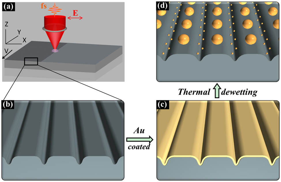
    Fig. 1. Schematic fabrication process of SERS substrates.
    (a) SEM image and (b) AFM profile of the surface morphology written on silicon samples. The scale bar represents 2 μm.
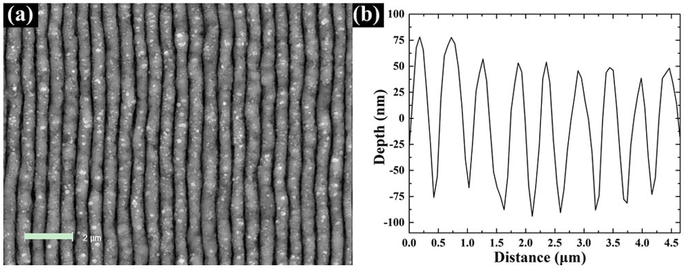
    Fig. 2. (a) SEM image and (b) AFM profile of the surface morphology written on silicon samples. The scale bar represents 2 μm.
    SEM images of NPs (a) on flat silicon surface and (c) on the ripple structure of 10 nm Au film dewetting; (b) and (d) are size distribution of NPs, respectively.
    Fig. 3. SEM images of NPs (a) on flat silicon surface and (c) on the ripple structure of 10 nm Au film dewetting; (b) and (d) are size distribution of NPs, respectively.
    (a) SERS spectra of different processing substrate. Red: FS+NPs area with 10−6 mol/L R6 G; Blue: FS + Film with 10−6 mol/L R6G; Green: NPs with 10−6 mol/L R6G; Black: fs laser-machined silicon with 10−2 mol/L R6G. (b) Raman map image of 20 μm×20 μm areas on the SERS substrates.
    Fig. 4. (a) SERS spectra of different processing substrate. Red: FS+NPs area with 106 mol/L R6 G; Blue: FS + Film with 106 mol/L R6G; Green: NPs with 106 mol/L R6G; Black: fs laser-machined silicon with 102 mol/L R6G. (b) Raman map image of 20μm×20μm areas on the SERS substrates.
    SERS spectrum on fs laser-machined, gold-coated, thermal dewetting substrates coating different thicknesses of films.
    Fig. 5. SERS spectrum on fs laser-machined, gold-coated, thermal dewetting substrates coating different thicknesses of films.
    EFs of SERS signal at 1361 cm−1 on fs laser-machined, gold-coated, thermal dewetting substrates coating different thicknesses of gold films. (a)–(e) scale bars represent 500 nm, (f) and (g) represent 200 nm.
    Fig. 6. EFs of SERS signal at 1361cm1 on fs laser-machined, gold-coated, thermal dewetting substrates coating different thicknesses of gold films. (a)–(e) scale bars represent 500 nm, (f) and (g) represent 200 nm.
    Xudong Tan, Lan Jiang, Jie Hu, Pengjun Liu, Andong Wang, Yong Lu. Highly sensitive and homogeneous SERS substrate fabricated by a femtosecond laser combined with dewetting[J]. Chinese Optics Letters, 2015, 13(11): 111401
    Download Citation