1Department of Applied Physics, Beihang University, Beijing 100191, China
2State Key Laboratory of Luminescence and Application, Changchun Institute of Optics, Fine Mechanics and Physics, Chinese Academy of Sciences, Changchun 130000, China
Yan Jia, Qingnan Yu, Fang Li, Mingqing Wang, Wei Lu, Jian Zhang, Xing Zhang, Yongqiang Ning, Jian Wu. Experimental investigation of loss and gain characteristics of an abnormal InxGa1-xAs/GaAs quantum well structure[J]. Chinese Optics Letters, 2018, 16(1): 011402
Copy Citation Text
In this Letter, the loss and gain characteristics of an unconventional asymmetrical step well structure consisting of variable indium contents of materials are measured and analyzed for the first time, to the best of our knowledge. This special well structure is formed based on the indium-rich effect from the material growth process. The loss and gain are obtained by optical pumping and photoluminescence (PL) spectrum measurement at dual facets of an edge-emitting device. Unlike conventional quasi-rectangle wells, the asymmetrical step well may lead to a hybrid strain configuration containing both compressive and tensile strains and, thus, special loss and gain characteristics. The results will be very helpful in the development of multiple wavelength InGaAs-based semiconductor lasers.
It has been well known that conventional quantum well lasers are designed and fabricated with a quasi-rectangle well structure at present, in which each well consists of a fixed content of material system, such as , , etc. In this case, the loss and gain characteristics of the quantum well can be well characterized by both theoretical and experimental methods[1–5]. These conventional quasi-rectangle quantum well lasers have been widely used in various industries[6–11]. However, the conventional well structure will also restrict further innovation in semiconductor lasers, such as widely tunable or multiple wavelength lasers.
If a quantum well consists of variable contents of a material system, its structure and characteristics may produce some interesting changes, which would be beneficial to the development of new types of lasers. is just such a material system with which an asymmetrical step well structure could be constructed. This is because in the material growth process, as indium atoms are migrating up to the surface of the layer, a number of indium-rich islands could be formed[12]. This would result in the reduction of indium content in the sub-surface of the material system, so that an unconventional asymmetrical step well structure consisting of variable contents of materials is formed. This is an interesting topic. Unfortunately, to the best of our knowledge, no articles have reported and investigated the loss and gain characteristics of such an abnormal well structure for the development of new lasers so far, since pure theoretical calculation for the asymmetrical step well structure is difficult.
Hence, in this Letter, we first produce an unconventional asymmetrical step well structure that is formed based on the indium-rich island effect. Then, the special loss and gain characteristics of the well are measured by acquiring the photoluminescence (PL) spectra from the dual facets of an edge-emitting device under optical pumping, where a new whole loss spectrum measurement approach for the abnormal well structure is proposed as well. Finally, the loss and gain characteristics are analyzed in detail.
Sign up for Chinese Optics Letters TOC. Get the latest issue of Chinese Optics Letters delivered right to you!Sign up now
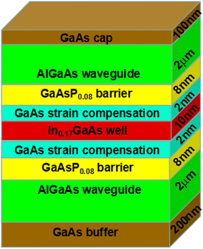
The theoretical quantum well structure is designed as follows. The device is 0.5 mm in width and 1.5 mm in length, which is grown on the GaAs substrate. The active layer consists of materials with a thickness of 10 nm here to obtain necessary indium-rich islands on the surface of the layer in the material growth process[13–16]. If the thickness of the InGaAs layer is thin and the indium content in InGaAs is low, there will not be any apparent indium-rich islands observed due to short migration length for indium atoms and low lattice mismatching[17,18]. The well is sandwiched by 2-nm-thick GaAs compensation layers. Beyond the GaAs compensation layers are the 8-nm-thick barriers. In the material growth process, the materials are deposited at 650°C with a growth rate of 0.08 nm/s. The pressure for the growth is 100 mbar and the V/III ratio is 350.
Since the indium content in the sub-surface of the layer will decrease[19], it leads to an asymmetrical well structure consisting of different indium contents of materials. A diagram of the well structure with indium-rich islands is illustrated in Fig. 1.
Figure 1.InGaAs/GaAs quantum well structure with indium-rich islands.
In order to measure the loss and gain of such an asymmetrical step well structure, the fiber-coupled 808 nm laser beam with a flat-top intensity profile is used to vertically pump the device and generate the uniform carrier distribution within the pumped region.
For optical loss measurement, we are describing a novel approach for the optically pumped asymmetrical InGaAs/GaAs well structure. The method is different from the previous techniques of using various carrier injection regions, because the use of various carrier injection regions would lead to errors in PL measurement, especially when the well contains randomly distributed indium-rich islands[1,3]. The method is based on the derivation of PL spectra from the dual facets of an edge-emitting device. The measurement principle is described in Fig. 2, in which both facets of the device are coated with reflectance of to allow spontaneous emission light only to singly pass the cavity without round trips. The actual reflectance of both coated facets is in the experiment. So, the errors from the reflectance can be ignored[5]. A mask with a 0.5-mm-wide slit is placed on the surface of the sample to guarantee a fixed pumping area. So, the whole absorption region of the sample is separated into two sections of , and .
Figure 2.Principle of the loss measurement based on the PL spectra from dual facets of an edge-emitting device.
Since a narrow region is pumped by the uniform pump light, the spontaneous emissions from both sides of the pumped region are identical in intensity. The spontaneous emission lights propagate toward two opposite directions and are attenuated because of internal scattering, free-carrier absorption, and inter-band optical absorption within the material system.
The PL spectral intensities of and at the dual mirrors of the edge-emitting device can be written as where is the optical loss coefficient. and are the propagation distances of the spontaneous emission lights from the pumped region. Thus, the loss coefficient can be obtained by combining Eqs. (1) and (2):
The PL intensities of and are measured and shown in Fig. 3. Unlike the usual PL spectrum with one peak from a conventional quantum well structure, two apparent peaks are observed in one PL spectral curve from our experiment. This should be interpreted by the indium-rich island effect. The double peaks in the PL spectra means that the well consists of different contents of materials.
Figure 3.(Color online) PL spectra measured at the dual facets of the sample pumped by a fiber-coupled 808 nm laser.
In terms of the model-solid theory[20], it is easy to work out that the double peaks in each curve are exactly corresponding to the indium contents of , and , respectively, for the material system. Thus, this forms an unconventional quantum well called a step well here. It consists of both and materials. To analyze this special well feature, the energy band structure of the well is drawn as Fig. 4.
Figure 4.Model of the energy band structure consisting of and materials.
The whole loss spectrum within the well is obtained using PL data and Eq. (3). The whole loss data are plotted in Fig. 5. Obviously, this loss curve characterizes the total absorption of the hybrid and material system, i.e., the absorption of the asymmetrical step well structure. In Fig. 5, the segment of A-E only indicates the absorption feature of the materials. However, the segment of E-I shows a hybrid absorption feature determined by both and materials, in which the materials play a dominant role.
Figure 5.Optical loss spectra of the hybrid and material system.
The hybrid step well structure leads to two absorption peaks in the loss curve, which are marked by D and H.
Based on the analysis on Fig. 4, it is found that the asymmetrical step well would lead to hybrid strains[21]. Since the lattice constant of the is bigger than that of the GaAs, the compressive strain occurs between the and GaAs layers. Meanwhile, a tensile strain may occur at the boundary of the and layers. These can be further illustrated by measuring the PL spectra in transverse electric (TE) and transverse magnetic (TM) polarizations and calculating the corresponding losses, respectively. The results are shown in Fig. 6.
Figure 6.(Color online) (a) PL spectra in TE polarization, (b) PL spectra in TM polarization, (c) the whole loss spectrum in TE polarization, and (d) the whole loss spectrum in TM polarization.
Figures 6(a) and 6(c) show that the TE photons that are generated and absorbed mainly come from the electron transition between the conduction band and heavy hole band. The double peaks in the curves emerge due to two different indium contents of and , which are next to each other in one well. In this case, the compressive strain between and GaAs layers leads to a heavy hole band higher than a light hole one for the materials, so the electron transitions happen between the conduction band and the heavy hole band.
In Figs. 6(b) and 6(d), the tensile strain between and materials in the well results in a light hole band higher than a heavy hole one for the materials so that electron transitions happen between the conduction band and the light hole band, and TM photons are generated and absorbed. The result shows that the space between the absorption peak J in Fig. 6(c) and the absorption peak N in Fig. 6(d) is 0.08 eV, while the space between the absorption peak K in Fig. 6(c) and the absorption peak M in Fig. 6(d) is 0.02 eV. These results agree well with the theoretical values given in Fig. 4.
The optical gain is obtained by measuring the PL spectra from the dual facets of the same edge-emitting device. In comparison with the model for the loss measurement described in Fig. 2, the difference only lies in that one facet is coated with a certain reflectance of rather than , and the other one is still coated as . The optical injection covers the whole surface of the device rather than a narrow local area. Based on above-described design, the modal gain can be expressed by[5]where is the active region length, is the reflectance of one facet, , , and are the PL intensities measured at both facets of the device, respectively.
The PL intensities of and in both TE and TM polarizations for the gain acquirement are measured at room temperature. The results are shown in Fig. 7, where the optical pump-induced carrier density is . The TE and TM gain spectra under various pump powers are obtained and shown in Fig. 8. In Fig. 8, both TE and TM gain curves show the double-peak configuration as well. This is apparently caused by to the abnormal step well structure.
Figure 7.PL spectra in TE and TM polarizations from the gain measurement sample, where the optical pump-induced carrier density is .
Figure 8 shows that the TE gain is obviously larger than the TM one for low energies of photons, while the TM gain is slightly larger than the TE one for high energies of photons. This is because there a compressive strain exists between the and GaAs layers. In this case, the calculated transition matrix elements in TE and TM polarizations are , and , respectively, in terms of the transition matrix elements theory[22]. Obviously, the result indicates that the TE gain is larger than the TM one. However, the tensile strain occurs between and materials due to the lattice constant of the being larger than that of . So, the transition matrix elements in TE and TM polarizations are calculated to be , and , respectively. This result shows that the TM gain would be slightly higher than the TE one, as the degeneracy is partially removed under a weak strain condition.
An interesting phenomenon from Fig. 8 is that as the carrier density is increased, the maximum of the TM gain, i.e., the main peak in the TM gain curve, rises a little faster than the main peak in the TE gain does. This can lead to the possibility of generating double-wavelength lasing with different polarizations for each wavelength of lasing. The lasing powers from both wavelengths would also be more identical to each other, as the peak gains in TE and TM polarizations will be near to the same level with increased carrier densities.
In conclusion, the optical losses and gains in both TE and TM polarizations are measured for an unconventional asymmetrical step quantum well structure, where a new experimental approach for the whole loss spectrum measurement is proposed in the Letter. The special double-peak formation and hybrid strain characteristics in both the loss and gain spectra due to the abnormal step well structure are analyzed based on the indium-rich islands effect and the transition matrix elements theory. The analysis on the gain measurement results show that such an asymmetrical step well structure and its gain characteristics will be helpful to generating new double-wavelength lasing with different polarizations for each wavelength of lasing. Meanwhile, the lasing powers from both wavelengths would also be more identical to each other.
Yan Jia, Qingnan Yu, Fang Li, Mingqing Wang, Wei Lu, Jian Zhang, Xing Zhang, Yongqiang Ning, Jian Wu. Experimental investigation of loss and gain characteristics of an abnormal InxGa1-xAs/GaAs quantum well structure[J]. Chinese Optics Letters, 2018, 16(1): 011402