• Chinese Physics B
  • Vol. 29, Issue 9, (2020)
Peng Fan1, Rui-Zi Zhang1, Jing Qi1, En Li1, Guo-Jian Qian1, Hui Chen1, Dong-Fei Wang1, Qi Zheng1, Qin Wang1, Xiao Lin1、2, Yu-Yang Zhang1、2, Shixuan Du1、2、†, Hofer W A1、3, and Hong-Jun Gao1、2
Author Affiliations
  • 1Institute of Physics and University of Chinese Academy of Sciences, Chinese Academy of Sciences (CAS), Beijing 0090, China
  • 2CAS Center for Excellence in Topological Quantum Computation, Beijing 100190, China
  • 3School of Natural and Environmental Sciences, Newcastle University, Newcastle upon Tyne Ne77RU, UK
  • show less
    DOI: 10.1088/1674-1056/abab80 Cite this Article
    Peng Fan, Rui-Zi Zhang, Jing Qi, En Li, Guo-Jian Qian, Hui Chen, Dong-Fei Wang, Qi Zheng, Qin Wang, Xiao Lin, Yu-Yang Zhang, Shixuan Du, Hofer W A, Hong-Jun Gao. Epitaxial synthesis and electronic properties of monolayer Pd2Se3[J]. Chinese Physics B, 2020, 29(9): Copy Citation Text show less
    Schematic diagrams of the fabrication process of monolayer Pd2Se3 and STM images. (a) The schematic diagram of the fabrication process. Firstly, Pd and Se atoms were deposited simultaneously with the substrate maintained at 500 K for 10 minutes (top panel). Bilayer PdSe2 was fabricated (middle panel). After annealed at selenium-deficient atmosphere, monolayer Pd2Se3 was successfully synthesized (bottom panel). (b) A large scale STM image (Vs = –1 V, It = 10 pA) of Pd2Se3. The inset is the line-profile cross the step edge, highlighted by the black dashed line. (c) A zoom-in STM image (Vs = –1 V, It = 100 pA) of Pd2Se3 and line-profile cross the patterns. The inset shows simulated STM image (Vs = –0.8 V). Scale bar: 0.5 nm. The lattice constants are 0.60 nm in a direction and 0.61 nm in b direction.
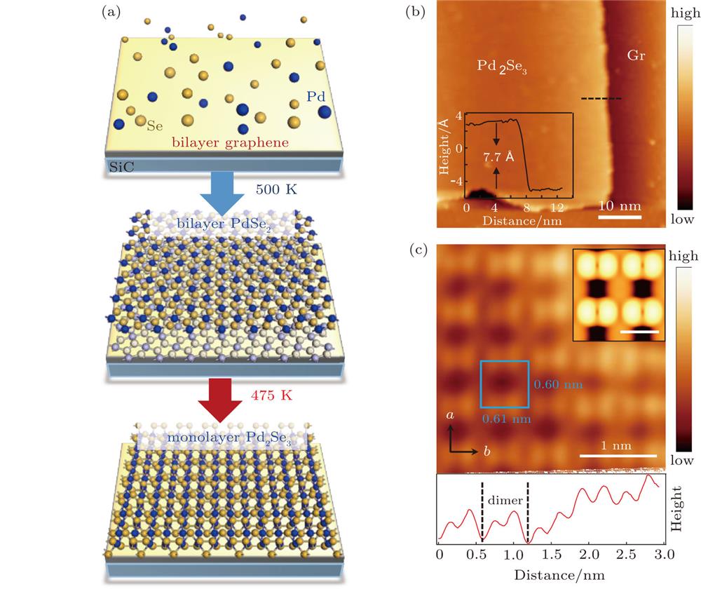
    Fig. 1. Schematic diagrams of the fabrication process of monolayer Pd2Se3 and STM images. (a) The schematic diagram of the fabrication process. Firstly, Pd and Se atoms were deposited simultaneously with the substrate maintained at 500 K for 10 minutes (top panel). Bilayer PdSe2 was fabricated (middle panel). After annealed at selenium-deficient atmosphere, monolayer Pd2Se3 was successfully synthesized (bottom panel). (b) A large scale STM image (Vs = –1 V, It = 10 pA) of Pd2Se3. The inset is the line-profile cross the step edge, highlighted by the black dashed line. (c) A zoom-in STM image (Vs = –1 V, It = 100 pA) of Pd2Se3 and line-profile cross the patterns. The inset shows simulated STM image (Vs = –0.8 V). Scale bar: 0.5 nm. The lattice constants are 0.60 nm in a direction and 0.61 nm in b direction.
    The atomic structure and electronic properties of monolayer Pd2Se3. (a) A high-resolution AFM image (A = 100 pm, Z = –4.5 Å) of monolayer Pd2Se3. A model of the topmost layer is superimposed on the image. The red ellipse highlights Se–Se dimer, which is higher than undimerized Se atoms. (b) Side-view, top-view, and front-view of monolayer Pd2Se3. (c) d I/d V spectra (red line (Vs = –1 V, It = 100 pA)) and the calculated density of states (blue line) of monolayer Pd2Se3.
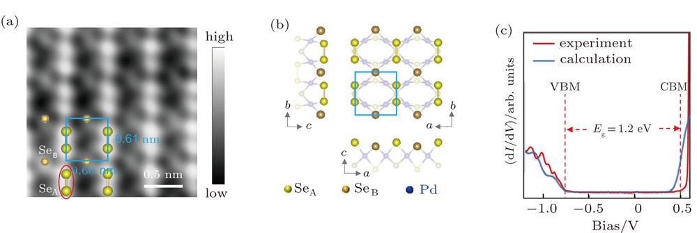
    Fig. 2. The atomic structure and electronic properties of monolayer Pd2Se3. (a) A high-resolution AFM image (A = 100 pm, Z = –4.5 Å) of monolayer Pd2Se3. A model of the topmost layer is superimposed on the image. The red ellipse highlights Se–Se dimer, which is higher than undimerized Se atoms. (b) Side-view, top-view, and front-view of monolayer Pd2Se3. (c) d I/d V spectra (red line (Vs = –1 V, It = 100 pA)) and the calculated density of states (blue line) of monolayer Pd2Se3.
    The atomic structure of the Se vacancy in monolayer Pd2Se3. (a) and (b) The STM images (It = 100 pA) of Se vacancies at the sample bias voltages of –1 V and 1 V, respectively. The butterfly-like and pitlike structures are Se vacancies. (c) An atomic-resolution AFM image (A = 100 pm, Z = –4.5 Å) containing a Se vacancy. The red dashed circle highlights one Se vacancy. (d) DFT calculated structure of a Se vacancy. The red dashed circle corresponds to the one shown in panel (c). The black dashed circles indicate the Se–Se dimer before Se vacancy forms. When one of the Se atoms disappears, the other moves to the position of the red dot and binds to the four neighboring Pd atoms.
    Fig. 3. The atomic structure of the Se vacancy in monolayer Pd2Se3. (a) and (b) The STM images (It = 100 pA) of Se vacancies at the sample bias voltages of –1 V and 1 V, respectively. The butterfly-like and pitlike structures are Se vacancies. (c) An atomic-resolution AFM image (A = 100 pm, Z = –4.5 Å) containing a Se vacancy. The red dashed circle highlights one Se vacancy. (d) DFT calculated structure of a Se vacancy. The red dashed circle corresponds to the one shown in panel (c). The black dashed circles indicate the Se–Se dimer before Se vacancy forms. When one of the Se atoms disappears, the other moves to the position of the red dot and binds to the four neighboring Pd atoms.
    Electronic properties of Se vacancy. (a) An STM image (Vs = –1 V, It = 10 pA) of Se vacancy. (b) and (c) Waterfall plots of a period normalized STS (Vs = –1 V, It = 100 pA) along the green arrow and the red arrow in panel (a), respectively. The black dashed lines indicate the gap edge at the valance band. P1 (the grey dashed line), P2 (the green dashed line), and P3 (the blue dashed line) indicate three main defect levels. (d) The dI/dV map (Vs = –1 V, It = 100 pA) at –0.6 V of Se vacancy. The corresponding region is highlighted by dashed blue box in panel (a).
    Fig. 4. Electronic properties of Se vacancy. (a) An STM image (Vs = –1 V, It = 10 pA) of Se vacancy. (b) and (c) Waterfall plots of a period normalized STS (Vs = –1 V, It = 100 pA) along the green arrow and the red arrow in panel (a), respectively. The black dashed lines indicate the gap edge at the valance band. P1 (the grey dashed line), P2 (the green dashed line), and P3 (the blue dashed line) indicate three main defect levels. (d) The dI/dV map (Vs = –1 V, It = 100 pA) at –0.6 V of Se vacancy. The corresponding region is highlighted by dashed blue box in panel (a).
    Peng Fan, Rui-Zi Zhang, Jing Qi, En Li, Guo-Jian Qian, Hui Chen, Dong-Fei Wang, Qi Zheng, Qin Wang, Xiao Lin, Yu-Yang Zhang, Shixuan Du, Hofer W A, Hong-Jun Gao. Epitaxial synthesis and electronic properties of monolayer Pd2Se3[J]. Chinese Physics B, 2020, 29(9):
    Download Citation