Abstract
In this study, a full-color emission red–green–blue (RGB) quantum-dot (QD)-based micro-light-emitting-diode (micro-LED) array with the reduced optical cross-talk effect by a photoresist mold has been demonstrated. The UV micro-LED array is used as an efficient excitation source for the QDs. The aerosol jet technique provides a narrow linewidth on the micrometer scale for a precise jet of QDs on the micro-LEDs. To reduce the optical cross-talk effect, a simple lithography method and photoresist are used to fabricate the mold, which consists of a window for QD jetting and a blocking wall for cross-talk reduction. The cross-talk effect of the well-confined QDs in the window is confirmed by a fluorescence microscope, which shows clear separation between QD pixels. A distributed Bragg reflector is covered on the micro-LED array and the QDs’ jetted mold to further increase the reuse of UV light. The enhanced light emission of the QDs is 5%, 32%, and 23% for blue, green, and red QDs, respectively.1. INTRODUCTION
As a low-power-consumption, low-cost, and highly luminous light source, gallium-nitride-based light-emitting diodes (LEDs) have attracted much attention, where applications include visible light communications [1–11], vehicle headlights [12,13], and backlight units (BLU) in liquid crystal displays (LCDs) [14–19]. Furthermore, micro-LEDs with micrometer-scale () sizes have different properties from the large-scale (scale of a few hundred micrometers) LEDs, such as high current density operation and thus high optical power density [20]. By fabricating the micro-LEDs into an array, they can function as a high-brightness, high-quality BLU in an LCD display. However, in order to achieve the full-color display, red–green–blue (RGB) light-emitting units should be distributed on the same panel, which is difficult to realize by epitaxial or fabrication effort. Such an issue can be overcome by using an alternative emitting source of colloidal quantum dots (QDs) and exciting the QDs optically by the LEDs [21]. QDs have attracted much attention, particularly because of the large-area color gamut than can be achieved with their narrow linewidths. In our previous research [22], a full-color emitting panel is achieved by combining RGB QDs with micro-UV micro-LEDs of pixel size and in arrays. In common, the light utilization efficiency of the LCD display system is caused mostly by the loss by the LCD backlight system. Use of a photoluminescence (PL) QDs display can replace the color filters and with a very large color gamut (1.52 times that of NTSC 1976). Color gamut was an evaluation metric, which was determined by the maximum colors in the display. A new color triangle was devised to strictly define the color gamut standard, which is called Rec. 2020. Our previous research demonstrated a QD microdisplay with over 80% of the color gamut of Rec. 2020 [23]. To accurately locate QDs on the micro-LED array, the aerosol jet (AJ) technique was used as the key technology to realize such a QD-LED display. However, our previous results also showed that, even with the optimized AJ parameters, the cross-talk effect still occurred during the QD deposition due to the overflow of QDs during the solvent evaporation.
In this work, we demonstrate a significant reduction in the cross-talk effect during the AJ printing process by using a photoresist (PR)-defined mold with a blocking wall to confine QDs. Furthermore, by adding a distributed Bragg reflector (DBR), the utilization of UV light can be more effective due to the fact that the reflected UV light can be reabsorbed by QDs, and the issue of human body safety can also be explored.
2. RESULTS AND DISCUSSION
Figure 1(a) shows the schematic illustration of an AJ system, which is developed by the Optomec Corporation. As described in Section 3, the QDs in the solvent are atomized in an ultrasonic atomizer and then transferred to the nozzle to jet the QDs. Regarding the QDs used in this study and similar to our previous research, CdSe QDs were purchased from the UT Dots Corporation, and the average sizes of the QDs are , , and for blue, green, and red QDs, respectively. Figure 1(b) shows the PL of the colloidal QDs used in this study; the emission wavelength covers the spectrum from red (630 nm), to green (535 nm), to blue (450 nm).
Sign up for Photonics Research TOC. Get the latest issue of Photonics Research delivered right to you!Sign up now
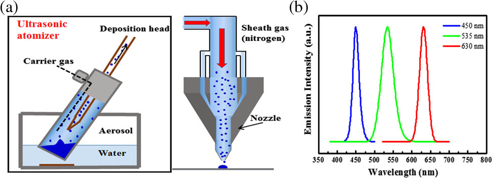
Figure 1.(a) Schematic illustration of the AJ system. (b) The PL emission spectra of QDs with emission wavelengths of 450, 535, and 630 nm.
Before the QDs are printed on micro-LEDs, Fig. 2 shows the National Chiao Tung University (NCTU) pattern printed by AJ red QDs, where the linewidth is examined via an OM and a fluorescence microscope simultaneously, as shown in Figs. 2(a) and 2(b), respectively. The resulting linewidth is confirmed that it can be well controlled at about 14 and 35 μm. However, the heights of the QDs have a corresponding change with linewidth. As shown in Fig. 2(c), for linewidths of 14.3 and 33.2 μm, the heights of the jetted QDs are 0.44 and 3.75 μm, respectively. For the small linewidth, the emission intensity would be too weak. As a consequence, the linewidth is limited to 30–40 μm.

Figure 2.AJ red QD NCTU pattern observed by (a) optical microscopy, (b) fluorescence microscopy, and (c) the measured height of the deposited red QD by laser microscopy.
The micro-LED array used in this study is similar to the one in our previous work [22], with an emission wavelength of 395 nm, a single pixel size of , and a pitch of 40 μm. The total array number is in a chip area of . The UV micro-LED is chosen instead of the blue micro-LED because the RGB QDs have higher quantum yields in the UV region than in blue region. In order to reduce the optical cross-talk effect in the previous work, a mold with open windows and blocking walls was fabricated by a PR and using the simple lithography technique. The window size here is the same as the micro-LEDs, and the unopened region forms the blocking wall that is just the shape of the trench between micro-LEDs, as shown in Fig. 3(a). The window size is about with a pitch of 40 μm, which is the same as the micro-LED array. Figure 3(b) shows the laser scanner microscope image of the PR mold, and the height of the PR wall is 11.46 μm. The PR mold was fabricated by the photolithography process by the AZ 5214-E (from MicroChem). The definition of the mask for the PR mold fabrication was modulated with a similar pitch size as for the micro-LED array—this was convenient to align in the followup. The PR mold covering may reduce the cross talk of QDs, and the sidewall was silver coated to reflect the leakage of light from the sidewall and prevent new cross talk from occurring.
Figure 3.(a) Optical microscopy image of PR square windows with the pixel size of , where the pitch is about 40 μm. (b) The laser scanner microscope image of the PR square wall, where the height of the wall is 11.46 μm.
Figure 4(a) shows that the UV passive-matrix micro-LED arrays were fabricated on UV epiwafers with a peak wavelength of 395 nm and a pitch size of 40 μm. The micro-LED pixels fabricated in the same column share a common electrode of the n-type GaN. All of the stripes of the micro-LED array have been created as isolation trenches via dry etching of GaN down to the sapphire substrate. By the dry etching process, was used as the hard mask. Finally, the p-electrode stripes were defined on top of the chips, the n-electrode stripes were defined on the n-GaN layer, and then a connection was made to all of the pixels in the same row. By aligning the windows of the mold to the micro-LED mesa, as shown in Figs. 4(b)–4(e), the AJ RGB QDs can be effectively deposited on the micro-LED mesa region but prevent overlap with the trench region. In order to fit the window size, the printing parameters are optimized. The adjustable parameters include the working distance between the nozzle and the substrate, the carrier gas flow rate, the sheath gas flow rate, and the stage speed. Table 1 summarizes the optimized parameters. The working distance and stage speed are fixed due to the fact that it might cause too wide of a range of change. Hence, in our case, only the carrier gas flow rate and the sheath gas flow rate are changeable. The concentrations of the RGB QDs in this study are controlled in the same condition. However, the RGB QDs were with different particle sizes because the wavelengths of the QDs were modulated by the particle sizes. The size-dependent properties of the QDs will alter the deposition condition of the AJ system. As a result, different flow rates are needed to control of the AJ system. Usually, we need to increase the carrier gas flow rate as the particle size grows. At the same time, when the carrier gas increases, the flow rate of sheath gas needs to increase as well to hold the linewidth of the deposited QDs, which is about 35 μm in this study.
Figure 4.Process flow of the full-color microdisplay. (a) The structure of the micro-LED arrays. (b) Aligning the mold to the UV micro-LED array. (c)–(e) Consequently jetting the RGB QDs inside the mold window to form the full-color pixels.
| QD Wavelength (nm) | Working Distance (mm) | Carrier Gas Flow Rate (sccm) | Sheath Gas Flow Rate (sccm) | Stage Speed (mm/s) |
| 630 | 1 | 83 | 17 | 10 |
| 535 | 1 | 72 | 15 | 10 |
| 450 | 1 | 66 | 11 | 10 |
Table 1. Parameters of the AJ Printing Technique for Different QDs
Before the RGB QDs are jetted, alignment between the PR mold and the micro-LED array was necessary. Alignment between the PR mold and the micro-LED array was performed by an X–Y stage system and an optical microscope (OM). The PR mold was fabricated by the photolithography process, and the definition of the mask was modulated to be suitable for the micro-LED array. The X–Y stage system used in this study was with 1 μm resolution, and then we placed the micro-LED array in a sticking position and observed the alignment process in the OM image. We defined an alignment cross in a sticking position of the micro-LED array, as shown in Fig. 5(a). Next, we focused on the PR mold in the OM image and moved the PR mold to align the alignment cross, as shown in Figs. 5(b)–5(c). Finally, the PR mold was pasted on top of the micro-LED array, thereby completing the alignment process.
Figure 5.Alignment approach. (a) The OM image focused on the micro-LED array and the defined alignment cross in a sticking position. Parts (b) and (c) show the OM image focused on the PR mold and the location moved to align the alignment cross, respectively.
After the deposition of QDs on the UV micro-LEDs via AJ and window-confined PR mold, the RGB pixel of the micro display has been demonstrated. Figure 6(a) shows the OM image of the well-deposited QDs on the micro-LEDs, which are isolated from the adjacent region. To further investigate the QD distribution characteristics, fluorescence microscopy was conducted. The result shown in Fig. 6(b) reveals that the light-emitting region from the QDs has a clear boundary. Compared to the AJ printing result without a PR mold, as shown in Fig. 6(c), the fluorescence image shows that no clear separation between printed QDs can be seen. It is obvious that the cross-talk phenomenon has been observed in the blue QD line while the green and red QD lines have been aggressed by blue QD line. The top-view image of the microdisplay in our previous research is shown in Fig. 7(b) [22]. The red line depicts the overlap of the blue and green lines, which caused the cross-talk effect to induce the pixels with a color shift. Cross talk has been defined as a metric to express how much of the value is obtained for a particular display system, which is referred to as Wood’s research [24]. The cross-talk value is defined by where “Leakage” is the luminance of light that leaks from the unintended channel to the intended channel, which is defined as the overlap area. We find that the intended channel is about 40.2 μm, as shown in Fig. 7(a). The overlap area of the red line for the previous design in Fig. 6(b) is about 13.4 μm (the deviation between 53.4 and 40.2 μm). The cross-talk value of the previous design is about 32.8%. The PR mold can limit the QD area in the intended channel, and with the silver coating to reflect the leakage of light from the sidewall, as shown in Fig. 7(c), it means that a lower cross-talk value (near zero) has been demonstrated in this study.
Figure 6.(a) Microscope image of the full-color micro-LED after jetted QDs in the PR mold. (b) The RGB pixel array observed by fluorescence microscopy. (c) The fluorescence microscopy image of the jetted QD pixels without the PR mold.
Figure 7.(a) Top-view image of the micro-LED layout with the pitch of 40.2 μm defined as the intended channel. (b) Our previous work by the QD lines without the PR mold for the microdisplay, which caused cross talk. (c) The QD droplets jetted in the PR mold to confine the size and resolve the cross-talk effect.
On the other hand, a spot pattern could waste QDs. Based on calculations, the material costs of (area of ) is about 9.7 nL of red QDs, 18.8 nL of green QDs, and 21.8 nL of blue QDs. We believe that the design of a PR layer can reduce material costs for a large-area microdisplay for the mass production process in the future.
This study resolves the coffee ring effect by the PR layer for our micro-LED. The significant coffee ring effect means that the ring-like QD particles deposit along the perimeter and with a pinhole when the QD droplets dry on a solid surface. At the perimeter, evaporation of the liquid is swifter than at the middle because the perimeter has a thinner thickness than the middle. However, the height profile must maintain the spherical cap shape dictated by surface tension and needs to prevent shrinkage [25–27]. The QD solution must flow outward, and then the QD particles were brought to the perimeter by the solution during evaporation. The QD particles were deposited along the perimeter to produce a coffee ring, where the mechanism is as shown in Fig. 8(a). Figure 8(c) shows that the OM image of the GaN substrate with QD drops, which was observed to produce the coffee ring effect. The mechanism of the PR mold to resolve the coffee ring effect is as shown in Fig. 8(b). The mold has been designed to control similar liquid thickness in the perimeter site and the middle site by confining the solution. A similar liquid thickness would cause similar rapid evaporation, which could prevent the QD particles from being brought to the perimeter or middle site by the solution. Figure 8(d) illustrates that QD drops could be confined in the hole, thereby resolving the coffee ring effect.
Figure 8.(a) Mechanism of the coffee ring effect due to the QDs’ outward flow during evaporation. (b) Mechanism of the solution to reduce the coffee ring effect by the PR mold. (c) The OM image denoted that the coffee ring effect can be observed when the QD drops were jetted on the GaN substrate. (d)The PR square can confine the QD drops in the hole and resolve the coffee ring effect.
In order to increase the UV light utilization, and avoid biological damage, a DBR structure has been designed for the microdisplay. The DBR structure is prepared via alternative deposition of 17.5 pairs of multilayers on a quartz glass. The measured reflectance of the DBR is shown in Fig. 9(a). The stop-band width and stop center of of the DBR is 80 and 395 nm, respectively. The maximum reflectance of the DBR is 92.5% at 395 nm. The DBR structure was composed of multiple pairs of different refractive index dielectric layers to achieve higher reflectivity in the selected wavelength. The basic equation to design the DBR structure is where is the selected wavelength, the thickness of the stacking dielectric materials depends on the refraction index and incidence angle , is the number of stacked layers, and , , and represent the refractive indices of the substrate and the stacking dielectric layers, respectively [28,29]. After covering the prepared DBR on the QDs-deposited LED array, the measured electroluminescence (EL) spectrum shown in Fig. 9(b) reveals that the light output from the QDs is enhanced by 23%, 32%, and 5% for red, green, and blue, respectively. The relative small enhancement in blue QDs is due to the unoptimized DBR reflectance at 450 nm, which is comparatively higher than the DBR reflectance for green and red QDs, as shown in Fig. 9(a). This can be further improved by designing the DBR layer stack with a layer thickness of . Two rows of the RGB pixels have been driven, and this enables individual addressable excitation of each pixel, as shown in Fig. 10(a). The difference brightness of each pixel is caused by the leakage current from the micro-LED array; we will resolve this problem in the future. Figure 10(b) demonstrates the full-color micro-LED in full operation and with the DBR layer covered.
Figure 9.(a) Reflectance spectrum of 17.5 pairs of the DBR. (b) The measured EL spectrum of jetted RGB QDs by AJ on a UV micro-LED array, where the black and red lines represent the devices with and without the DBR, respectively.
Figure 10.(a) A row of the RGB pixel has been driven individual addressable. (b) The full-color micro-LED in full operation and with the DBR layer covered.
To estimate the conversion efficiency of the RGB QDs used in our microdisplay, we defined the optical conversion efficiency (OCE) to calculate the ratio of the energy transfer. The colloidal QD degradation can be incorporated in the OCE evaluation via the following equation: where and are the integrated emission intensities in the visible band of the spectrum with and without QDs, and and are the integrated intensities excited by UV light with and without QDs, respectively [30,31]. By calculation, the OCE of the blue, green, and red micro-LED is about 2.25% for blue light, 10.8% for green light, and 6.9% for red light. The reason for the lower OCE values is that in the absence of protected fabrication, the QDs would decrease most of the efficiency by the influence of moisture, oxidation, and heat. We will design any protected structure to optimize reliability in the future.
Figure 11 illustrates the microdisplay in operation to drive the single to yield red, green, and blue light, individually. The luminance of blue, green, and red emission that was driven individually by the RGB micro-display is about for a single red pixel, for a single green pixel, and for a single blue pixel, respectively. Most indoor LCD displays have brightness values in the range of , and our microdisplay had a luminance of in full color, which is enough for display applications.
Figure 11.Images of the full-color microdisplay in operation to individually drive the (a) single blue pixel, (b) single green pixel, and (c) single red pixel.
3. MATERIALS AND METHODS
A. Fabrication of the UV Micro-LED Array
The epitaxial structure of the UV micro-LED was grown by metal organic chemical-vapor deposition, which consists of an undoped GaN buffer layer on a sapphire substrate, followed by n-GaN, a multiple quantum well with a peak emission wavelength of 395 nm, p-GaN, and a current-spreading layer (CSL) for metal contact. The UV micro-LED array was fabricated as follow: mesa dry etching down to n-GaN via inductively coupled plasma (ICP), p-metal deposition on the CSL, n-metal deposition on the n-GaN layer, and then the trench opened by ICP etching down to the sapphire substrate in order to isolate each micro-LED from each other, and sidewall passivation by plasma-enhanced chemical vapor deposition-deposited .
B. AJ System
The aerosol system consisted of two major parts: an ultrasonic atomizer and a spraying chamber. First, the RGB QDs with concentrations of in solvent were prepared in a tube that is inside the ultrasonic atomizer, and then the suspension was atomized by the ultrasonic vibration. The resulting AJ was consequently transferred to the nozzle by nitrogen gas flow. After the nitrogen gas input, the AJ was tightly focused at the end of nozzle to produce small drops, enabling narrow linewidth and high resolution.
4. CONCLUSION
In conclusion, we demonstrated a full-color microdisplay with a composite of a UV micro-LED array and RGB QDs by using the AJ technique, whereby the linewidths of the QDs could be well controlled to fit the sizes of micro-LEDs. Furthermore, a mold was made by simple lithography to reduce the optical cross-talk effect, the QDs were jetted into the window of the mold with clear separation between each pixel. A DBR provided a more efficient utilization of UV light and enhanced the QD emission intensity by 23%, 32%, and 5% for red, green, and blue, respectively. With these techniques, high-quality microdisplays can be achieved.
Acknowledgment
Acknowledgment. The authors would like to thank the Electronic and Optoelectronic System Research Laboratories of the Industrial Technology Research Institute and the Ministry of Science and Technology of Taiwan for their financial support.
References
[1] T. Komine, M. Nakagawa. Fundamental analysis for visible-light communication system using LED lights. IEEE Trans. Consum. Electron., 50, 100-107(2004).
[2] Y. Wang, Y. Wang, N. Chi, J. Yu, H. Shang. Demonstration of 575-Mb/s downlink and 225-Mb/s uplink bi-directional SCM-WDM visible light communication using RGB LED and phosphor-based LED. Opt. Express, 21, 1203-1208(2013).
[3] Y. Wang, N. Chi, Y. Wang, L. Tao, J. Shi. Network architecture of a high-speed visible light communication local area network. IEEE Photon. Technol. Lett., 27, 197-200(2015).
[4] J. Vučić, C. Kottke, S. Nerreter, K. Habel, A. Büttner, K.-D. Langer, J. W. Walewski. 230 Mbit/s via a wireless visible-light link based on OOK modulation of phosphorescent white LEDs. Optical Fiber Communication Conference, OThH3(2010).
[5] C. Chow, C. Yeh, Y. Liu, Y. Liu. Improved modulation speed of LED visible light communication system integrated to main electricity network. Electron. Lett., 47, 867-868(2011).
[6] C. Yeh, Y. Liu, C. Chow, Y. Liu, P. Huang, H. Tsang. Investigation of 4-ASK modulation with digital filtering to increase 20 times of direct modulation speed of white-light LED visible light communication system. Opt. Express, 20, 16218-16223(2012).
[7] F.-M. Wu, C.-T. Lin, C.-C. Wei, C.-W. Chen, Z.-Y. Chen, K. Huang. 3.22-Gb/s WDM visible light communication of a single RGB LED employing carrier-less amplitude and phase modulation. Optical Fiber Communication Conference, OTh1G. 4(2013).
[8] Z. Wang, C. Yu, W.-D. Zhong, J. Chen, W. Chen. Performance of a novel LED lamp arrangement to reduce SNR fluctuation for multi-user visible light communication systems. Opt. Express, 20, 4564-4573(2012).
[9] W.-Y. Lin, C.-Y. Chen, H.-H. Lu, C.-H. Chang, Y.-P. Lin, H.-C. Lin, H.-W. Wu. 10m/500Mbps WDM visible light communication systems. Opt. Express, 20, 9919-9924(2012).
[10] H. Le Minh, D. O’Brien, G. Faulkner, L. Zeng, K. Lee, D. Jung, Y. Oh, E. T. Won. 100-Mb/s NRZ visible light communications using a postequalized white LED. IEEE Photon. Technol. Lett., 21, 1063-1065(2009).
[11] D. Tsonev, H. Chun, S. Rajbhandari, J. J. McKendry, S. Videv, E. Gu, M. Haji, S. Watson, A. E. Kelly, G. Faulkner. A 3-Gb/s single-LED OFDM-based wireless VLC link using a gallium nitride micro-LED. IEEE Photon. Technol. Lett., 26, 637-640(2014).
[12] I. Takai, T. Harada, M. Andoh, K. Yasutomi, K. Kagawa, S. Kawahito. Optical vehicle-to-vehicle communication system using LED transmitter and camera receiver. IEEE Photon. J., 6, 1-14(2014).
[13] C.-C. Hsieh, Y.-H. Li, C.-C. Hung. Modular design of the LED vehicle projector headlamp system. Appl. Opt., 52, 5221-5229(2013).
[14] C.-Y. Wu, T.-F. Wu, J.-R. Tsai, Y.-M. Chen, C.-C. Chen. Multistring LED backlight driving system for LCD panels with color sequential display and area control. IEEE Trans. Ind. Electron., 55, 3791-3800(2008).
[15] C.-C. Chen, C.-Y. Wu, Y.-M. Chen, T.-F. Wu. Sequential color LED backlight driving system for LCD panels. IEEE Trans. Power Electron., 22, 919-925(2007).
[16] D. Cho, W.-S. Oh, G. W. Moon. A novel adaptive dimming LED backlight system with current compensated XY channel drivers for LCD TVs. J. Display Technol., 7, 29-35(2011).
[17] Y.-K. Lo, K.-H. Wu, K.-J. Pai, H.-J. Chiu. Design and implementation of RGB LED drivers for LCD backlight modules. IEEE Trans. Ind. Electron., 56, 4862-4871(2009).
[18] H. Cho, O.-K. Kwon. A local dimming algorithm for low power LCD TVs using edge-type LED backlight. IEEE Trans. Consum. Electron., 56, 2054-2060(2010).
[19] H.-J. Chiu, Y.-K. Lo, T.-P. Lee, S.-C. Mou, H.-M. Huang. Design of an RGB LED backlight circuit for liquid crystal display panels. IEEE Trans. Ind. Electron., 56, 2793-2795(2009).
[20] J. Herrnsdorf, J. J. McKendry, S. Zhang, E. Xie, R. Ferreira, D. Massoubre, A. M. Zuhdi, R. K. Henderson, I. Underwood, S. Watson. Active-matrix GaN micro light-emitting diode display with unprecedented brightness. IEEE Trans. Electron Devices, 62, 1918-1925(2015).
[21] K. J. Chen, H. C. Chen, K. A. Tsai, C. C. Lin, H. H. Tsai, S. H. Chien, B. S. Cheng, Y. J. Hsu, M. H. Shih, C. H. Tsai. Resonant‐enhanced full‐color emission of quantum‐dot‐based display technology using a pulsed spray method. Adv. Funct. Mater., 22, 5138-5143(2012).
[22] H.-V. Han, H.-Y. Lin, C.-C. Lin, W.-C. Chong, J.-R. Li, K.-J. Chen, P. Yu, T.-M. Chen, H.-M. Chen, K.-M. Lau. Resonant-enhanced full-color emission of quantum-dot-based micro-LED display technology. Opt. Express, 23, 32504-32515(2015).
[23] R. Zhu, Z. Luo, H. Chen, Y. Dong, S.-T. Wu. Realizing Rec. 2020 color gamut with quantum dot displays. Opt. Express, 23, 23680-23693(2015).
[24] A. J. Woods. Crosstalk in stereoscopic displays: a review. J. Electron. Imaging, 21, 040902(2012).
[25] R. D. Deegan, O. Bakajin, T. F. Dupont, G. Huber, S. R. Nagel, T. A. Witten. Capillary flow as the cause of ring stains from dried liquid drops. Nature, 389, 827-829(1997).
[26] C. Jiang, Z. Zhong, B. Liu, Z. He, J. Zou, L. Wang, J. Wang, J. Peng, Y. Cao. Coffee-ring-free quantum dot thin film using inkjet printing from a mixed-solvent system on modified ZnO transport layer for light-emitting devices. ACS Appl. Mater. Interfaces, 8, 26162-26168(2016).
[27] S.-W. Wang, H.-Y. Lin, C.-C. Lin, T. S. Kao, K.-J. Chen, H.-V. Han, J.-R. Li, P.-T. Lee, H.-M. Chen, M.-H. Hong. Pulsed-laser micropatterned quantum-dot array for white light source. Sci. Rep., 6, 23563(2016).
[28] I. García, J. Geisz, M. Steiner, J. Olson, D. Friedman, S. Kurtz. Design of semiconductor-based back reflectors for high Voc monolithic multijunction solar cells. 38th IEEE Photovoltaic Specialists Conference (PVSC), 002042(2012).
[29] H. K. H. Choy. Design and fabrication of distributed Bragg reflectors for vertical-cavity surface-emitting lasers. IEEE International Conference on Semiconductor Electronics(1998).
[30] K. Suzuki, A. Kobayashi, S. Kaneko, K. Takehira, T. Yoshihara, H. Ishida, Y. Shiina, S. Oishi, S. Tobita. Reevaluation of absolute luminescence quantum yields of standard solutions using a spectrometer with an integrating sphere and a back-thinned CCD detector. Phys. Chem. Chem. Phys., 11, 9850-9860(2009).
[31] S. C. Hsu, Y. H. Chen, Z. Y. Tu, H. V. Han, S. L. Lin, T. M. Chen, H. C. Kuo, C. C. Lin. Highly stable and efficient hybrid quantum dot light-emitting diodes. IEEE Photon. J., 7, 1-7(2015).


