Abstract
An effective and simple method is proposed for fabricating the micro/nano hybrid structures on metal surfaces by adjusting femtosecond laser fluence, scanning interval, and polarization. The evolution of surface morphology with the micro/nano structures is discussed in detail. Also, the mechanism of light absorption by the micro/nano hybrid structures is revealed. Compared with the typical periodic light-absorbing structures, this type of micro/nano hybrid structures has an ultralow average reflectivity of 2% in the 250–2300 nm spectral band and the minimum 1.5% reflectivity in UV band. By employing this method, large areas of the micro/nano hybrid structures with high consistency could be achieved.1. Introduction
Light absorption surfaces on metal are of both fundamental interest and realistic values in various fields, such as aerospace, solar cells, artificial blackbodies, infrared imaging, and so on. Due to the problems of interface bonding and thermal expansion coefficient differences between the film and substrate, traditional technologies such as black anodizing and sandblasting encounter difficulties, such as oxide layer peeling off, poor blackening consistency, and limited light absorption capacity and service life. Compared with the traditional chemical methods, the fabrication of micro/nano structures on metal surfaces for antireflection has the advantages of high reflectivity and stable performance. Various techniques have been proposed to produce regulated antireflective micro/nano structures on metal surfaces, such as chemical etching[1], mechanical grooving[2], reactive ion etching[3], and long-pulse laser processing[4].
Due to its simplicity, flexible machining of space, high processing accuracy, and environmental friendliness, ultrafast laser manufacturing technology is one of the relatively ideal manufacturing technologies for fabricating light-trapping structure surfaces with antireflection[5–8]. By employing an ultrafast laser, black or colored metals (e.g., aluminum, gold, platinum, tungsten, copper, titanium, and stainless steel) were obtained, the typical reflectivity of which was around 5%–15% from the UV to near infrared (NIR) spectrum range[9–20].
It is possible to achieve a lower reflectivity by means of optimizing the laser processing parameters or combining with other technologies[6,21–32]. For example, Iyengar et al. reported the fabrication of textured metal surfaces by ultrafast laser processing, whose reflection combined with scattering could be reduced to 3% over the spectral range from 404 nm to 1550 nm[29]. Zheng et al. achieved the titanium alloy surface with the reflectivity as low as 2.43% in a wide range from 200 nm to 2600 nm by an ultrafast laser assisted with chemical fluorination treatment[7]. Fan et al. proposed a general ultrafast laser direct writing strategy for fabricating highly effective antireflection structures on different metal surfaces[17]. Combining the femtosecond (fs) laser with the nanosecond laser, Lou et al. achieved an average reflectivity of 3.1% in the 250 nm to 2250 nm spectral band on the titanium alloy surface[30]. Ding et al. fabricated sequential color surfaces on copper by adjusting the laser defocusing distance, the sequential evolution tendency and corresponding mechanism of which were conducted[31]. However, fewer studies have been reported to simply and effectively achieve broadband effectiveness and ultralow average reflectivity performance on metal surfaces.
Sign up for Chinese Optics Letters TOC. Get the latest issue of Chinese Optics Letters delivered right to you!Sign up now
In this study, we proposed an effective and simple way for fabricating the micro/nano hybrid structures on metal surfaces by adjusting fs laser parameters. The effect of laser fluence, scanning interval, and polarization on the surfaces’ morphology and average reflectivity was studied. The evolution and formation of the micro/nano structures were discussed in details. Also, the mechanism of light absorption by the micro/nano hybrid structures is revealed. Compared with the typical periodic light-absorbing structures, this type of micro/nano hybrid structure has an ultralow metal reflectivity in a wide spectral range.
2. Experimental Setup
A TC7 titanium alloy sample with a size of was used in our experiments. The mechanically polished surface of the sample was cleaned in an ultrasonic cleaner with anhydrous ethanol and deionized water before laser treatment. For metal surface modification, an industrial fs laser (Pharos-20 W from Light Conversion, Lithuania) with a high repetition rate (1 MHz) and the highest power (20 W) was employed. The pulse width of the ultrafast laser system was 290 fs at a wavelength of 1030 nm. An galvanometric scanner (Scanlab, Germany) was used to control the laser beam and was focused by a telecentric field mirror (Lenstek Laser Optics, China). The scanning head was mounted on a axis (Aerotech, USA), and the defocusing distance could be controlled by adjusting the distance of the axis. The laser polarization was converted from linear polarization to circular polarization through a 1/4 wave plate (Thorlabs, USA). The diameter of the focused spot defined by the intensity drops to of the maximum value was approximately 20 µm. The three-dimensional morphology of the micro/nano structures induced by the fs laser on the surface of the metal was characterized by a scanning electron microscope (SEM) of tungsten filament (Japan), two field emission scanning electron microscopes (Hitachi, Japan), and a confocal microscopy (Keyence, Japan), respectively. The reflectance of laser-treated Ti samples from the UV to the NIR region (250–2300 nm) was measured using a spectrophotometer (integrating sphere was used as spectrometer accessory) (Shimadzu Corporation, Japan).
3. Results and Discussion
During the process of fs laser blackening metal, low repetition rate or low pulse energy with low processing efficiency is frequently used[17,29]. The industrial fs laser with a high repetition rate and high power was employed to solve this problem. Table 1 presents the calculated laser fluence for the single pulse energy from 100 µJ to 400 µJ. It is much higher than the ablation threshold of of titanium alloy[33]. In the case of N pulses due to high spot overlapping rate, the actual fluence would be expanded thousands of times and is much greater than the damage threshold at the focal plane[33–35]. This factor leads to the extremely high thermal melting effect caused by the metal heat accumulation, which then results in a large amount of laser-melted ejections. Figure 1 exhibits images of micro/nano structures of the samples fabricated by the fs laser at the focal plane, where the laser fluence, scanning speed, and repetition frequency were , 50 mm/s, and 50 kHz, respectively. The hot melting and resolidification region formed a close arrangement of columnar structures, which had less optical cavity micro/nano structures. With the generation of columnar structures, the surface became gray, the color of which was uneven, as shown in Fig. 1.

Figure 1.Images of micro/nano structures fabricated by the fs laser at the focal plane. The laser power and scanning speed were 20 W and 50 mm/s, respectively.
| Pulse Energy (µJ) | Repetition Frequency (kHz) | Laser Fluence (J/cm2) |
|---|
| 100 | 50 | 32 (single pulse) |
| 200 | 50 | 64 (single pulse) |
| 300 | 50 | 95 (single pulse) |
| 400 | 50 | 127 (single pulse) |
Table 1. Calculated Fluence of fs Laser at Different Pulse Energy
Firstly, the effect of defocusing distance on the surface morphology was investigated. As the laser repetition rate, power, scanning speed, and interval were fixed at 50 kHz, 20 W, 50 mm/s, and 30 µm, respectively, the change of defocusing distance brought about a variation of laser beam diameter on the surface of the processed samples and, accordingly, altered the pulse peak fluence and the total amount of pulses within a laser spot size (the accumulated fluence profile[33–35] and the pulse overlapping were both considered). The morphology of micro/nano structures is induced by the fs laser at different defocusing distances as displayed in Fig. 2. The accumulated fluence within a laser spot decreased sharply from to (the pulse peak fluence was changed from to ) with the defocusing distance increased from 0 to 1.60 mm. The pulses accumulated fluence declined rapidly, which caused the quick weakening of the laser material interaction and reduced the melting effect, forming micro grooves with a small amount of micro holes at the bottom of the material, as shown in Fig. 2(a). Then, as the defocusing distance increased from 1.60 mm to 1.66 mm, the fluence at the overlapped area was not high enough to form micro grooves, but to corral structures regularly distributed in the horizontal direction [Fig. 2(b)]and eventually evolved to an irregular hybrid micro/nano structure [Fig. 2(c)]. Also, the micro structures became hybrid structures with many kinds of micro pores, along with the calculated pulse peak fluence further decreased, as presented in Fig. 2(d). For the case of the defocusing distance further increased to 1.68 mm, the fluence decreased to a relatively low range, the micro/nano structures were still a hybrid distribution, but the morphology gradually became shallow holes according to Fig. 2(e).
Figure 2.Morphology of micro/nano structures induced by the fs laser at different defocusing distances: (a) 1.60 mm; (b) 1.62 mm; (c) 1.64 mm; (d) 1.66 mm; (e) 1.68 mm.
The changes of surface morphology fabricated by the fs laser at different defocusing distances ultimately lead to the difference in the sample’s reflectivity. Figure 3 illustrates the reflection spectra of the samples fabricated by the fs laser at different defocusing distances. Compared with 4.78% for the sample with micro grooves on the surface, the average reflectivity of the sample fabricated at 1.64 mm defocusing distance was nearly 3.43% in the spectra range from 250 nm to 2300 nm. As the defocusing distance further increased to 1.66 mm, the average reflectance continued to decrease to 3.19%, due to further hybridization of the micro/nano structure and a significant increase in the number of micro/nano structures as deep as 78 µm. It indicates that the hybrid micro/nano structures have better light absorption effects than the periodic distribution. This phenomenon could be explained by the geometric light trapping effect[8,17]. The randomly distributed large hollows, protrusions, and deep holes embedding architecture could effectively collect the incident light in a broad spectrum from all directions. However, due to the continuous decrease of the fluence incident on the sample surface with the increase of the defocusing distance, the depth and number of the processed micro structures had a sharp decrease. Therefore, the average reflectivity increased to 3.65%. Furthermore, different from the reflectance curvature change of other defocusing distances, the reflectivity for the sample in the case of 1.64 mm had a huge peak in the spectral band between 250 nm and 600 nm. By comparing the morphology fabricated at the different defocusing distances, the nanostructures for the case of 1.64 mm defocusing distance were quite different from others. It is believed that the morphology of the nanostructure has an important influence on the reflectivity at a specific wavelength as well as the average reflectivity.
Figure 3.Reflection spectra of the samples fabricated by the fs laser at different defocusing distances.
In order to further reduce the reflectivity of the titanium alloy sample, the effect of laser scanning intervals on surface morphology and reflectivity was conducted. The sample was placed 1.66 mm from the focal plane; at the scanning speed of 50 mm/s, repetition frequency of 50 kHz, and single pulse energy of 400 µJ,the scanning interval was increased from 20 µm to 50 µm.
Because the overlapping of the laser spot along the horizontal direction was unchanged, the micro/nano structure was still the hybrid irregular distribution, which contained micro holes, protrusions, cavities, etc., as exhibited in Fig. 4. However, the arrangement period, number, and depth of micro/nano structures need to be further studied.
Figure 4.SEM images of micro/nano hybrid structures fabricated by the fs laser at different scanning intervals: (a) 50 µm; (b) 40 µm; (c) 30 µm; (d) 20 µm.
The scanning interval of the laser only changed the overlapping rate of the spot in the vertical direction; assuming two laser spots with diameter D overlapped by interval L from the point of geometry, it is not difficult to find that the overlapping rate of them is . The interval changed from 50 µm to 40 µm, leading to the spot overlapping rate slightly increasing from 78.1% to 82.5%. Thus, strong interaction between incident laser pulses and material would happen under enough laser fluence, and there was significant increase in depth of the micro/nano structure, which increased from 69 µm to 81 µm. But, the overlapping rate was arbitrarily close to 91.2% when the scan interval rose to 20 µm continually. Thus, the scanning interval here was largely overlapped, and the massive accumulation of energy raised the temperature within the laser-irradiated region. There more violent ablation happened, which intensified the hydrodynamic process of the molten pool and weakened the resolidification of the micro/nano structure. The above process caused the depth of the micro/nano structure to become smaller to 74 µm, even if there existed more micro structures, as illustrated in Fig. 5.
Figure 5.Three-dimensional morphology of hybrid micro/nano structures with different scanning intervals: (a) 50 µm; (b) 40 µm; (c) 30 µm; (d) 20 µm.
Figure 6 exhibits the reflection spectra of the samples fabricated by the fs laser at different scanning intervals. It can be observed that the reflection levels of the samples with different laser scanning intervals exhibited different degrees of reduction. The average reflectance of the sample with a scanning interval of 50 µm was merely lower than 3.58% over the wavelength ranging from 250 nm to 2300 nm. When the scanning interval was decreased to 40 µm, the reflection of the sample was further inhibited to be less than 2.61% throughout the UV-VIS-NIR spectrum range, as the deeper hybrid micro/nano structure was obtained at the scanning interval of 40 µm, as presented in Fig. 5. Additionally, when the scanning interval was further decreased to 20 µm, the reflectance showed a certain increase to 3.36%, attributed to the depth of the micro structure becoming smaller, even if there existed a larger number of micro structures. Therefore, the final reflectivity of samples was the balance between the number and depth of micro structures. In addition, it should be noted that although the average reflectivity for the case of 40 µm was the lowest, it was much higher in the UV band than that of the other cases.
Figure 6.Reflection spectra of the samples fabricated by the fs laser at different scanning intervals.
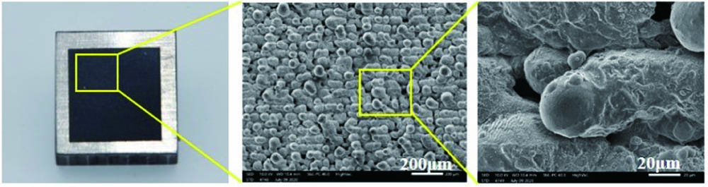
In addition, the influence of laser polarization on TC7 surface morphlogy and reflectivity was studied, as distributed in Figs. 7 and 8, respectively. Compared with the micro/nano structures processed by the linear polarized laser in Fig. 5, when the scanning interval, repetition frequency, and defocusing distance were all fixed, a large number of densely distributed protrusions and smaller apertures were generated in the case of the circularly polarized laser. It was observed that the number of circularly polarized pulses (10–30) needed to form micro/nano structures is higher than that of linearly polarized pulses (5–15)[36,37]. Since the total amount of circularly polarized laser pulses per spot was smaller than that of the linearly polarized laser pulses under the same laser parameters, the density of protrusions was reduced, while a large number of micro cavities with large openings emerged (Fig. 7). Attributed to the laser polarization changing the energy distribution of each pulse, the energy in the overlapping area had corresponding decreases, which resulted in the increase of the maximum micro holes’ depth from 81 µm to 88 µm. Finally, circularly polarized light is more conducive to the formation of laser induced periodic surface structures, of which more nano cavities and nano protrusions were generated. As for the overall antireflection performance, an average reflectivity of 2.0% was achieved, and the minimum reflectivity was 1.5% in the UV band, as displayed in Fig. 8. It also should be noted that the reflectivity of the samples processed by the circularly polarized laser has been greatly suppressed in the short wave range, which is due to the improvement of nanostructures[17,33].
Figure 7.Blackened sample fabricated by the circularly polarized laser and its morphology.
Figure 8.Reflection spectra of the samples fabricated by linearly and circularly polarized fs lasers, respectively.
The samples were also measured by X-ray diffraction (XRD) to check the chemical composition of samples. The evidence for oxide metal elements such as TiO (PDF#04-006-1902), (PDF#04-004-6417), and (PDF#00-003-1122) was found on the surface of the micro/nano structure, which was produced by the reaction since the TC7 ablation by the laser is done in air. From the test, the oxygen content was slight and not directly proportional to the reflectivity of the samples. Therefore, we believe that the laser induced black TC7 and its high absorption capacity are mainly attributed to the hybrid micro/nano structure formed on the surface, rather than the characteristics presented by other chemical productions. This point is also consistent with the conclusions described in many previous studies[6,14,16,24,38].
The mechanism of optical absorption of micro/nano hybrid structures fabricated by the circularly polarized laser is revealed in Fig. 9. Firstly, according to practical applications, the light absorption structures should meet the Lambert light source. Compared with the regularly distributed micro/nano structures, the distribution and opening of the hybrid micro/nano structures are disordered, which is conducive to the absorption of light from all directions into the optical cavity. For a single micro structure, the light absorption obeys the Fresnel reflection law[17,31]. Compared with the deep holes with smaller aperture, the cavities and deep holes with larger aperture are conducive to trap more beams into the optical cavity. Then, the light is reflected multiple times in the cavity, the energy of which becomes weak until it is blocked or absorbed by the internal rough nanostructures. Moreover, the nanostructures modified by circularly polarized light play an important role in reducing the spectral reflectivity. The abundant nano protrusions and cavities improve the surface roughness, which effectively reduces the intrinsically large optical impedance mismatch between metals and free space[17]. Lastly, the nanostructures generated by circularly polarized light are particularly important in reducing the reflectivity at specific wavelengths. According to the absorption principle of periodic nanostructures, the smaller the fringe period is, the better the resonance absorption of the short wave is. Since the hybrid nanostructure induced by circularly polarized light has a smaller fringe period, it has an excellent absorption of the short wave.
Figure 9.Mechanism of optical absorption of micro/nano hybrid structures processed by the circularly polarized laser.
4. Conclusions
In summary, we propose an efficient and simple strategy for the fabrication of micro/nano hybrid structures on metal surfaces by controlling fs laser processing parameters. Three-dimensional morphology and average reflectivity of the samples fabricated by the fs laser at different laser fluences, scanning intervals, and polarizations were discussed. Explanation for the formation of the micro/nano structures and light absorption mechanism was given. It is experimentally demonstrated that (1) the morphology of the samples fabricated by the fs laser changed greatly under different laser processing parameters; (2) an ultralow average reflectivity of 2% in the 250–2300 nm spectral band and minimum 1.5% reflectivity in UV band could be achieved. Due to its advantages of simplicity and high efficiency, this method could be applied to the fabrication of light absorption metal surfaces with large areas and high consistency for practical applications.
References
[1] P. Panek, M. Lipinski, J. Dutkiewicz. Texturization of multicrystalline silicon by wet chemical etching for silicon solar cells. J. Mater. Sci., 40, 1459(2005).
[2] M. Spiegel, C. Gerhards, F. Huster, W. Jooss, P. Fath, E. Bucher. Industrially attractive front contact formation methods for mechanically V-textured multicrystalline silicon solar cells. Sol. Energy Mater Sol. Cells., 74, 175(2002).
[3] J. Yoo, G. Yu, J. Y. Mater. Black surface structures for crystalline silicon solar cells. Mater. Sci. Eng. B, 159–160, 333(2009).
[4] L. A. Dobrzanski, A. Drygala, K. Golombek, P. Panek, E. Bielanska, P. Zieba. Laser surface treatment of multicrystalline silicon for enhancing optical properties. J. Mater. Process., 201, 291(2008).
[5] A. A. Ionin, Y. M. Klimachev, A. Y. Kozlov, S. I. Kudryashov, A. E. Ligachev, S. V. Makarov, L. V. Seleznev, D. V. Sinitsyn, A. A. Rudenko, R. A. Khmelnitsky. Direct femtosecond laser fabrication of antireflective layer on GaAs surface. Appl. Phys. B, 111, 419(2013).
[6] A. Y. Vorobyev, C. Guo. Femtosecond laser blackening of platinum. J. Appl. Phys., 104, 053516(2008).
[7] B. Zheng, W. Wang, G. Jiang, K. Wang, X. Mei. Fabrication of broadband antireflective black metal surfaces with ultra-light-trapping structures by picosecond laser texturing and chemical fluorination. Appl. Phys. B, 122, 180(2016).
[8] H. Huang, L. M. Yang, S. Bai, J. Liu. Blackening of metals using femtosecond fiber laser. Appl. Opt., 54, 324(2015).
[9] A. Y. Vorobyev, A. N. Topkov, O. V. Gurin, V. A. Svich, C. Guo. Enhanced absorption of metals over ultrabroad electromagnetic spectrum. Appl. Phys. Lett., 95, 121106(2009).
[10] A. Y. Vorobyev, C. Guo. Metallic light absorbers produced by femtosecond laser pulses. Adv. Mech. Eng., 2, 452749(2010).
[11] Y. H. Taek, A. Y. Vorobyev, C. Guo. Enhanced efficiency of solar-driven thermoelectric generator with femtosecond laser-textured metals. Opt. Express, 19, A824(2011).
[12] G. Tang, A. C. Hourd, A. Abdolvand. Nanosecond pulsed laser blackening of copper. Appl. Phys. Lett., 101, 231902(2012).
[13] H. Tao, X. Song, Z. Hao, J. Lin. One-step formation of multifunctional nano- and microscale structures on metal surface by femtosecond laser. Chin. Opt. Let., 13, 061402(2015).
[14] J. Fu, H. Liang, T. Zhang, Y. Wang, Y. Liu, Z. Zhang, X. Lin. Enhanced optical absorbance and fabrication of periodic arrays on nickel surface using nanosecond laser. Opt. Commun., 389, 170(2017).
[15] H. P. Wang, Y. C. Guan, H. Y. Zheng, M. H. Hong. Controllable fabrication of metallic micro/nano hybrid structuring surface for antireflection by picosecond laser direct writing. Appl. Surf. Sci., 471, 347(2019).
[16] G. Li, J. Li, C. Zhang, Y. Hu, X. Li, J. Chu, W. Huang, D. Wu. Large-area one-step assembly of 2.5-dimensional porous metal micro/nanocages by ethanol-assisted femtosecond laser irradiation for enhanced antireflection and hydrophobicity. ACS Appl. Mater. Interfaces, 7, 383(2015).
[17] P. Fan, B. Bai, M. Zhong, H. Zhang, J. Long, J. Han, W. Wang, G. Jin. A general strategy towards dual-scale controlled metallic micro-nano hybrid structures with ultralow reflectance. ACS Nano, 11, 7b03673(2017).
[18] B. W. Wu, C. Wang, Z. Luo, J. H. Li, S. Man, K. W. Ding, J. A. Duan. Controllable annulus micro/nanostructures on copper fabricated by femtosecond laser with spatial doughnut distribution. Chin. Opt. Lett., 18, 013101(2020).
[19] T. Chen, W. Wang, T. Tao, A. Pan, X. Mei. Multi-scale micro-nano structures prepared by laser cleaning assisted laser ablation for broadband ultralow reflectivity silicon surfaces in ambient air. Appl. Surf. Sci., 509, 145182(2020).
[20] T. Chen, W. Wang, T. Tao, X. Mei, A. Pan. Deposition and melting behaviors for formation of micro/nano structures from nanostructures with femtosecond pulses. Opt. Mater., 78, 380(2018).
[21] C. Florian, R. Wonneberger, A. Undisz, S. V. Kirner, K. Wasmuth, D. Spaltmann, J. Krüger, J. Bonse. Chemical effects during the formation of various types of femtosecond laser-generated surface structures on titanium alloy. Appl. Phys. A, 126, 266(2020).
[22] H. Tao, J. Lin. Enhancing microwave absorption of metals by femtosecond laser induced micro/nano surface structure. Opt. Lasers. Eng., 114, 31(2019).
[23] J. Wang, C. Guo. Formation of extraordinarily uniform periodic structures on metals induced by femtosecond laser pulses. J. Appl. Phys., 100, 023511(2006).
[24] P. X. Fan, M. L. Zhong, L. T. Huang, H. J. Zhang. Rapid fabrication of surface micro/nano structures with enhanced broadband absorption on Cu by picosecond laser. Opt. Express, 21, 11628(2013).
[25] J. Cheng, C. Liu, S. Shang, D. Liu, W. Perrie, G. Dearden, K. Watkins. A review of ultrafast laser materials micromachining. Opt. Laser. Technol., 46, 88(2013).
[26] A. Samanta, Q. Wang, G. Sing, S. K. Shaw, F. Toor, A. Ratner, H. Ding. Nanosecond pulsed laser processing turns engineering metal alloys antireflective and superwicking. Opt. Laser. Eng., 34, 260(2019).
[27] D. V. Ta, A. Dunn, T. J. Wasley, R. W. Kay, J. Stringer, P. J. Smith, C. Connaughton, J. D. Shephard. Nanosecond laser textured superhydrophobic metallic surfaces and their chemical sensing applications. Appl. Surf. Sci., 357, 248(2015).
[28] K. Ding, C. Wang, Y. Zheng, Z. Xie, Z. Luo, S. Man, B. Wu, J. Duan. One-step fabrication of multifunctional fusiform hierarchical micro/nanostructures on copper by femtosecond laser. Surf. Coat. Technol., 367, 244(2019).
[29] V. V. Iyengar, B. K. Nayak, M. C. Gupta, J. Liu. Ultralow reflectance metal surfaces by ultrafast laser texturing Laser. Appl. Opt., 49, 5983(2010).
[30] R. Lou, G. Zhang, G. Li, X. Li, Q. Liu, G. Cheng. Design and fabrication of dual-scale broadband antireflective structures on metal surfaces by using nanosecond and femtosecond lasers. Micromachine, 1, 11(2020).
[31] K. Ding, M. Li, C. Wang, N. Lin, H. Wang, Z. Luo, J. Duan. Sequential evolution of colored copper surface irradiated by defocused femtosecond laser. Adv. Eng. Mater., 22, 201901310(2020).
[32] C. Mauclair, D. Pietroy, Y. D. Maïo, E. Baubeau, J. P. Colombier, R. Stoian, F. Pigeon. Ultrafast laser micro-cutting of stainless steel and PZT using a modulated line of multiple foci formed by spatial beam shaping. Opt. Lasers Eng., 67, 212(2015).
[33] K. M. T. Ahmmed, C. Grambow, A. M. Kietzig. Fabrication of micro/nano structures on metals by femtosecond laser micromachining. Micromachines, 5, 1219(2014).
[34] K. M. T. Ahmmed, E. J. Y. Ling, P. Servio, A. M. Kietzig. Introducing a new optimization tool for femtosecond laser-induced surface texturing on titanium, stainless steel, aluminum and copper. Opt. Lasers Eng., 66, 258(2015).
[35] J. Eichstädt, G. R. B. E. Römer, A. J. Huis in 't Veld. Determination of irradiation parameters for laser-induced periodic surface structures. Appl. Surf. Sci., 264, 79(2013).
[36] K. Kurselis, R. Kiyan, B. N. Chichkov. Formation of corrugated and porous steel surfaces by femtosecond laser irradiation. Appl. Surf. Sci., 258, 8845(2012).
[37] B. K. Nayak, M. C. Gupta. Ultrafast laser-induced self-organized conical micro/nano surface structures and their origin. Opt. Lasers Eng., 48, 966(2010).
[38] T. Yong, H. Wang, A. Y. Vorobyev, C. Guo. Formation of solar absorber surface on nickel with femtosecond laser irradiation. Appl. Phys. A, 108, 299(2012).