Abstract
Topological insulators represent a new quantum phase of matter with spin-polarized surface states that are protected from backscattering, exhibiting electronic responses to light, such as topological quantum phase transitions. However, the effects of high-frequency driving topological intrinsic systems have remained largely unexplored challenges experimentally for high-sensitivity terahertz detection. In this study, by integrating topological insulators with subwavelength metal antennas through micro-nano processing, a high-frequency terahertz detector with high sensitivity is proposed. The enhanced response originates from the asymmetric scattering of the surface electrons in the flakes induced by the terahertz wave. The device displays room-temperature photodetection with a responsivity of 192 mA/W and equivalent noise power of less than in the frequency range from 0.02 to 0.3 THz. These results pave the way for the exploitation of topological insulators for high-frequency operation in real-time imaging within long-wavelength optoelectronics.1. INTRODUCTION
The terahertz (THz) region of the electromagnetic spectrum ranging from 0.1 to 10 THz [1] is a spectral window with rich scientific opportunities and exhibits great promise in applications [2–4]. For example, in the field of investigating matter, THz spectroscopy serves as a unique tool because many molecules have structural absorption resonance at these frequencies [5]. THz waves can penetrate numerous commonly used dielectric materials, which are opaque for visible and mid-infrared light, making them a unique tool for defense and security systems [6]. In the field of electronics, the THz range constitutes the ultimate limit of operation for high-frequency electronics. However, this region has been considered the scientific gap in the electromagnetic spectrum [7]. One of the issues is the lack of sensitive THz detectors. Many optoelectronic detection technologies that are widely used in the visible and infrared regimes cannot be easily translated to this long-wavelength regime because THz photon energies are far below typical electronic interband transitions [8]. The need for a cryogenic system due to the few meV photon energy of the THz wave sets up obstacles for the miniaturization of THz detectors.
Two-dimensional (2D) materials have attracted great attention nowadays and can provide an excellent platform for realizing room-temperature THz detection. Consisting of only one or a few atomic layers, 2D material exhibits unique electronic and optical properties that are distinctively different from those of bulk counterparts, enabling widespread applications in electronics and optoelectronic devices [9,10]. Currently, THz detectors constituted by layered 2D materials such as graphene [11] and black phosphorus [12] have shown potential implementation of room-temperature detection capacity, while suffering from several drawbacks such as slow response speed and high manufacturing costs [13,14]. Topological insulators are a unique quantum material because of topologically protected metallic boundary surface states on insulating bulk states, demonstrating a number of fascinating electronic and optical properties, such as spin-momentum locking, high photo–thermal–electric conversion efficiency, and ultra-broadband plasmon excitations [15,16]. Antimony telluride () is a kind of typical topological insulator with a small bandgap (0.23 eV) and is widely used in thermoelectric devices [17] and photonic devices [18]. Due to the spin–orbit coupling and time-reversal symmetry lying in the surface plane [19], a low-energy dissipation transport mechanism for the carriers could be extremely useful for an optoelectronic device, especially for high-speed operation. The peculiar properties of the gapless surface states with a Dirac cone-shaped dispersion in topological insulators make them an ideal photoresponse material for long-wavelength detection. For example, Liu et al. have reported good device performance of a silicon-based single-crystal bismuth telluride () photoconductive detector, exhibiting responsivity of to near-infrared light at room temperature [20]. Zheng et al. presented a near-infrared photodetector based on topological insulator film grown by molecular beam epitaxy, showing an obvious sensitivity to 980 nm light illumination [21]. Subsequently, Tang et al. realized THz detection with high responsivity in both self-powered and biased modes at room temperature, with a performance of responsivity over 75 A/W and response time shorter than 60 μs in self-powered mode operation, providing more possibilities for THz detection [22]. In spite of considerable efforts, studies so far have proven materials to be very realistic candidates for required detection applications in the visible and near-infrared regions, but research related to the properties of topological surface states is relatively lacking compared with and materials in THz detection. Actually, the topological surface states of were experimentally demonstrated to be more robust than those of and , which have better potential applications in the THz field due to their weak antilocalization effect in the two helical surface states layer [23]. Thus, the significant improvement in responsiveness obtained by exploring topological insulators with attractive properties can make THz detection a more practical application.
In this work, we innovatively propose a method of THz detection based on a subwavelength bow-tie antenna structure; the experimental results show that the responsivities reach 29.1 mA/W at 0.03 THz, 88.4 mA/W at 0.12 THz, and 66.9 mA/W at 0.28 THz, and the noise equivalent power (NEP) is lower than 1.05, 0.35, and , respectively. Moreover, the responsivities of flakes integrated with multiple bow-tie antennas reach up to 72, 192, and 75 mA/W along different routes, respectively. This study suggests that fascinating applications can be engineered in the -based device platform for high-sensitivity, low-noise, and high-speed operation through the integration of functional materials and ingenious photonic design.
Sign up for Photonics Research TOC. Get the latest issue of Photonics Research delivered right to you!Sign up now
2. METHOD
A. Device Fabrication
The butterfly antenna structure was prepared on the silicon dioxide layer at the top of the silicon substrate by ultraviolet lithography photography technology (MA/BA6 Gen4), and the metal electrode () was deposited by high vacuum evaporation technology (Ei-5Z). The thin layer of was stripped from the bulk crystal by the mechanical stripping method.
B. Structure Characterization
The element analysis of the material was carried out by an energy dispersive spectroscopy (EDS) spectrum analyzer (Gemini500). The thickness of the material was characterized by an environmental atomic force microscope (AFM) (Cypher ES).
C. Device Measurements
We used semiconductor analyzer equipment (B2912A) to measure the electrical performance of the device in a variable bias mode, and then used a stable microwave source (Agilent 8257D) of a continuous low-energy photon wave and a frequency multiplier and locked amplification technology to suppress noise, which has the detection ability of ultra-low current accuracy. For the measurement of light response, different frequencies (0.03, 0.12, and 0.28 THz) are generated by the multiplier of the electronic source. For the photoresponse experiment, a 0.04 THz source based on a frequency multiplier is used. The THz source was obtained by a microwave source (Agilent E8257D, 0.02–0.04 THz) equipped with Virginia Diodes Inc. (VDI) multipliers (WR-2.8 and WR-9 Tripler), operating in the frequency range of 0.02–0.3 THz. A TK100 power meter was used to measure the power output of the THz source ( for 0.03 THz, for 0.12 and 0.28 THz). THz waves were modulated with a 1 kHz square wave signal to use locking techniques in the presence of DC offset and noise. We used MStarter 200 high-precision photocurrent scanning measurement equipment to carry out photocurrent mapping on the device, and the ZEM-3 device to measure the Seebeck coefficient. The upper and lower electrodes are composed of nickel metal, and a certain current passes through the upper and lower electrodes. The lower electrode includes a heating wire, which provides a temperature difference for the sample. The side needle consists of an R-type thermocouple to accurately measure temperature and voltage at two points on the sample. For imaging applications, two pairs of off-axis parabolic mirrors are used to focus the 0.1 THz beams on the detector, and an image is obtained by raster scanning the object at the beam focus, consisting of points with an integration time of 10 ms in each.
3. RESULTS AND DISCUSSION
Figure 1(a) schematically illustrates the atomic stacking sketch of the crystal structure, consisting of a quintuple layer with the sequence of Te (I)-Sb-Te (II)-Sb-Te (I) (yellow shaded area) along the direction. A triangular lattice in five layers along the top view of the direction has three distinct positions, denoted as A, B, and C. The 2D surface carriers make the elastic scattering asymmetric in response to the electric field due to its special point group of , while the point group symmetry of the bulk states is , possessing space inversion properties [24]. Bow-tie antenna integrated THz detectors have been realized by exploiting a combination of ultraviolet lithography, metal evaporation, and lift-off technology (see Section 2). The bias electrodes were patterned in the shape of a planar bow-tie antenna with a channel length of 6 μm to couple the detected THz radiation to the detector and provide a broadband response [25]. The antennas consisted of a 50 nm thick gold layer, followed by a 5 nm thick layer of chromium acting as an adhesive layer between the gold electrode and substrate. flakes were then mechanically exfoliated from bulk crystal using a standard adhesive tape technique and transferred to the gap of the bow-tie antenna. The distribution of Te and Sb elements characterized by EDS is uniform as shown in Fig. 1(b), and the atomic ratio of Sb and Te is around 1: 1.5, which conforms to the chemical stoichiometry of . The Raman spectra as shown in Fig. 1(c) further confirm the structural conformation and layers of multilayer exfoliated flakes. Three typical characteristic peaks , , and at 98, 127, and correspond to the three phonon vibration modes, respectively [26]. The AFM images of flakes demonstrate that the thickness of the microplate is about 85 nm with good flake uniformity in Fig. 1(d).
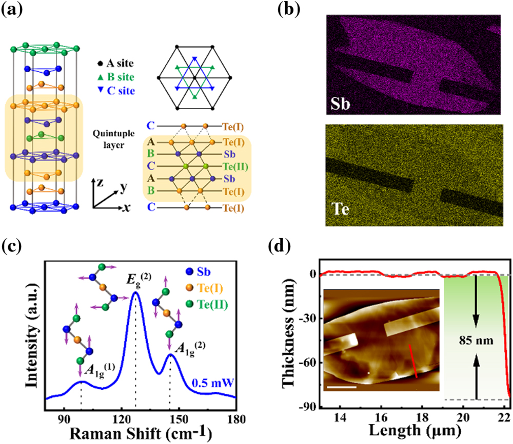
Figure 1.(a) Crystalline structure of ; corresponding top and side views are shown on the right. (b) EDS element mapping images for Sb and Te elements in flakes. (c) Raman spectrum of flakes excited by 514 nm laser with the power of 0.5 mW; inset shows the displacement patterns of , , and phonon modes. (d) Atomic force microscope scan image: the red line measurement area corresponds to the corresponding height map, and the scale bar is 6 μm.
Figure 2(a) schematically shows bow-tie antenna-integrated material detectors on the high-resistance silicon substrate for THz band detection at room temperature. The high-resistance silicon substrate was selected as the substrate because it is transparent to THz waves [27]. Numerical simulations by means of the finite-difference time-domain (FDTD) method were performed to evaluate the coupling enhancement of the incident THz wave at 0.03 THz. The incident THz wave is a transverse magnetic (TM) wave polarized for effective excitation of surface plasmon polaritons. The parameters of the bow-tie antenna are adopted from experimental values. As shown in the bottom panel of Fig. 2(a), the localized surface plasmon polaritons appear in the subwavelength structure, and the highest field enhancement occurs at the metallic–dielectric interface, with a magnitude 10 times larger than that of the incident wave. Then the electrical properties of these hybrid devices were characterized by studying the temperature-dependent current–voltage (I-V) curves [Fig. 2(b)] in a dark environment with a temperature ranging from 4 to 300 K. The dark current increases with temperature, which is in rough agreement with the special electronic structure where the Fermi level locates near the Dirac point [21]. The linear I-V curve shows Ohmic contact between the flakes and the gold electrodes with a resistance of 51.5 Ω at room temperature. Owing to its surface hosting gapless states with a linear energy dispersion, THz detection measurements are performed. The bow-tie antenna-coupled device is uniformly illuminated with a chopped THz beam generated by frequency multiplication technology (see Section 2 for details). Then, the open-circuit photovoltaic signal or short-circuit photocurrent signal of the material-based device is extracted by using a preamplifier, a lock-in amplifier, and a high-speed sampling oscilloscope. The selective frequency dependence of photoresponse from 0.02 to 0.30 THz is displayed in Fig. 2(c). The peak photocurrent of the -based device is around 6 μA, 400 nA, and 30 nA at a zero bias voltage under different radiation frequencies of 0.03, 0.12, and 0.28 THz with the average power of 30 mW. To understand the detection sensitivity of the designed device, the power density dependence of the photocurrent is explored, as expected, showing excellent linearity (), with the corresponding values of 0.9985, as shown in Fig. 2(d). The device exhibits a large dynamic modulation range by changing the bias voltage of the detector. Responsivity () of the detector is defined as the ratio of the output root mean square current to the average optical power incident on the detector, expressed as , where represents the generated photocurrent, is the incident THz power density, and is the sensitive area. To illustrate the time dynamics of this hybrid structure, the responsivity dependence of the modulation frequency shows that the photoresponse remains almost unchanged even if the modulation frequency increased to 10 kHz in Fig. 2(e). Additionally, the fast response speed of the photodetector is defined as the time required to rise from 10% to 90% on the rising edge or, analogously, the falling edge of photoresponse, as shown in Fig. 2(f). The rise time () and fall time () are determined to be about 21.5 and 20.5 μs, respectively, which are much faster than results reported previously [22], due mainly to the dissipation-less transport mechanism of the edge-state electrons in the surface state. The high responsivity and high-speed operation of this bow-tie antenna integrated topological insulator structure reveal an excellent photoelectric performance at the THz frequency band and its capability in video-rate imaging applications.

Figure 2.(a) Three-dimensional schematic diagram of terahertz detector. The electric field distribution of the -based device is shown in the bottom panel at 0.03 THz. (b) Typical current–voltage (I-V) curves in the temperature range of 4–300 K in a dark environment. (c) Terahertz spectral response of photodetector at zero bias voltage under radiation frequencies of 0.02–0.04, 0.07–0.12, and 0.24–0.30 THz with average power of 30 mW. (d) Photocurrent as a function of incident radiation power density () under different bias voltages. (e) Responsivity as a function of modulation frequency (Mod. Fre.) at a radiation frequency of 0.03 THz; inset shows time-resolved photoresponse at modulation frequencies of 1 and 5 kHz. (f) The time-resolved response for a single period shows a response time of . (g) Polarization dependence of photocurrent of the bow-tie antenna integrated devices at 0.03 THz. (h) Responsivities as a function of bias voltage under radiation frequencies of 0.03, 0.12, and 0.28 THz. (i) NEP and of the device under different radiation frequencies with error bars.
The high responsivity of the bow-tie integrated THz detector benefits from the broadband spectrum response and enhanced light–matter interaction originating from the excitation of the surface plasmon polaritons at the metallic–dielectric interface under a TM-polarized wave, shown in the bottom panel of Fig. 2(a) under 0.28 THz radiation. Therefore, this bow-tie integrated device features polarization-sensitive properties. Experimentally, the photocurrent dependence on polarization is illustrated in Fig. 2(g), when the device is illustrated by the THz wave at 0.03 THz. The photocurrent exhibits a lobe-like pattern with the ratio of maximum (polarization parallel to the slit) to minimum (polarization perpendicular to the slit) at about 1200, demonstrating the anisotropic properties of the device. Moreover, the bow-tie antenna integrated topological insulator device can also work in the bias mode. With the bias voltage traversing across the channel, the photogenerated carriers produce a drift current due to the Ohmic field at the biased junction, resulting in a symmetric and linear photocurrent–voltage relationship, which is consistent with previous studies [22,28], as shown in Fig. 2(h). The values of are 29.1, 88.4, and 66.9 mA/W at zero bias voltages at 0.03, 0.12, and 0.28 THz, respectively. When the bias voltage is increased to 50 mV, the corresponding can be further increased to 38.5, 106.5, and 86.1 mA/W, respectively. Our device responsivity is 1–2 orders of magnitude better than that of film/graphene [29] and heterojunction [30]. Note that the area of the antenna region is , far less than the THz light spot diffraction-limited region ( is the radiation wavelength); here our active detection regions , 0.50, and are taken to calculate responsivity at radiation frequencies of 0.03, 0.12, and 0.28 THz, respectively. Truthfully, the calculated responsivity of our device is grossly underestimated because the incident THz spot is much more than the sensitive region (or antenna region). The total noise of the device includes mainly flicker noise ( noise), shot noise (), and thermal noise (). Shot noise is caused by photo-generated carriers randomly in the detector under radiation or thermal excitation, and thermal noise generated by random thermal movement of carriers is related to Ohmic resistance and temperature. noise can be negligible because our equipment is efficient even under conditions of over 1 kHz at a zero bias voltage. So the main noise of our detectors includes shot noise and thermal noise, which can be defined as , where represents the Boltzmann constant, represents the absolute temperature of the detector in Kelvin, represents the resistance of the detector in Ohms, represents the basic charge, and represents the dark current of the detector (in this case, bias current); the calculation result is . Figure 2(i) shows the NEP and the normalized detection rate () calculated from the noise spectrum and . NEP is an important performance parameter for estimating the ability of the photodetectors to receive weak signals that can be calculated based on the ratio of , reaching 1.05 , 0.35, and at 0.03, 0.12, and 0.28 THz, respectively. The NEP of the photodetector is lower than that of flakes because of the much lower noise of our device [31]. can accurately reflect the ability of photoelectric detection materials to detect weak light, defined as . Our bow-tie integrated topological insulator THz detector can reach 0.83, 2.04, and at 0.03, 0.12, and 0.28 THz, respectively. Thus, our bow-tie antenna features high responsivity, high-speed operation, and broadband spectrum photoresponse characteristics.
We further characterized the intrinsic photoresponse of flakes to optimize photoelectric conservation performance. The Seebeck coefficient () of the materials was measured by the schematic diagram in Fig. 3(a). A certain current was passed to the sample through the upper and lower electrodes composed of nickel metal, in which the temperature range of the lower electrode is changeable from 36 to 300 K for the sample, and the upper electrode was kept at a constant temperature (see Section 2 for details). Figure 3(b) displays a significant increase with the temperature range from 36 to 300 K, indicating the thermoelectric properties of flakes as they depend on temperature. The Seebeck coefficient of at 300 K is 132 μV/K, showing that it is an analogous electronic state of Dirac materials with high carrier mobility for THz detection. An explanation for low-photon absorption, similar to graphene [32] and (absolute value) [33], is related to the low heat capacity associated with the massless Dirac electrons of graphene and topological surface states. As early as 2014, Olbrich et al. reported the photogalvanic effect (PGE) of the three-dimensional topological insulator during the research process [24]. In 2018, Plank and Ganichev reviewed experimental and theoretical studies of PGE generated by polarized THz radiation-based three-dimensional topological insulators [34]. By the FDTD method under 0.12 THz in Fig. 3(d), the photocurrent density related to the PGE exhibits symmetric distribution with respect to the two interfaces, while the photocurrent summed to zero, related to the photon-drag effect (PDE), has an asymmetric distribution. Thus, the photocurrent caused by the PGE of our device is much higher than by the PDE. When the THz radiation is applied to our detector, the net photocurrent is generated due to the asymmetric scattering of the wedge, violating the balance of the system. Thus, the direction of the current generated depends on the polarization of the incident electric field and the specific direction of the wedge. For example, when the electric field direction is parallel to the wedge base (horizontal direction), a photocurrent flowing in the -axis direction in the upper panel of Fig. 3(e) is generated, and when the electric field direction is rotated 90°, the current direction is reversed, generating the photovoltaic response with the current direction depending on the polarization of the incident THz waves. When a bias electric field is applied to the device, the generated photocarriers are accelerated and efficiently separated towards the ends of metallic contacts, and ultimately the photocurrent increases in the lower panel of Fig. 3(e). As a comparison experiment, from the spatial dependence of the photoresponse under the illumination of a 520 nm laser in Fig. 3(c), an existing mirror visible photocurrent of 207 nA near the interface electrodes can be clearly observed and complementarily canceled, illustrating the contact effects on visible photoresponse. Unlike the higher-energy photons excited in visible regions, the low-energy-photon response in our detector is closely related to the domination of the intraband absorption and PGE owing to the weak effect of material thickness on photoresponse [with the same order of magnitude under 0.1 THz radiation in Fig. 3(f)], enough to rule out contact effects.
Figure 3.(a) Schematic diagram of Seebeck coefficient test device. (b) Seebeck coefficient as a function of temperature range from 36 to 300 K. (c) Scanning photocurrent measurements of the photodetector under illumination of a 520 nm laser with a zero bias. (d) Display of the excitations under 0.12 THz excitation in a single device of photogalvanic effect and photon-drag effect along the plane. (e) Upper panel: PGE model excited on the surface state due to the asymmetry of elastic scattering caused by the wedge. Lower panel: scattered electrons are efficiently extracted under static bias field, leading to the enhanced photocurrent with bias mode. (f) Photoresponse dependence on the thickness of flakes under 0.1 THz radiation illumination.
Furthermore, we turn to characterize the photoresponse of flakes integrated with multiple bow-tie antennas as shown in Fig. 4(a). The near field of multiple bow-tie antenna pairs can shape 2D distributions of carriers to facilitate its nonuniform absorption along different routes, and a net photocurrent can be expected to flow in different directions. When the incident light polarization angle is 45° at 0.12 THz, the enhanced electric field is distributed symmetrically across the four electrodes as shown in the upper left panel in Fig. 4(a). Under visible light, the mirror photocurrent of the device with multiple contacts originates from the contact effect in Figs. 4(b) and 4(c), which are consistent with the discussion of the two-terminal detector above. The THz response of the device, tuned actively by THz polarization, originates from the contribution of topological surface states. We focus on the THz polarization dependence photocurrent a few μA larger than mirror photocurrent and 49 nA of visible light, guiding the electromagnetic radiation normally to the device after the polarization rotator. The THz beam size was much larger than the device size to ensure the uniformity of the power intensity illuminated on the device. Linearly polarized light with an electric field oriented along different angles from 0° to 360° was used to explore the intrinsic response of the device along the A/C route in . The photocurrent dependence on the polarization angle shows the sinusoidal function relationship, further demonstrating the asymmetrical scattering-based operation principle [Fig. 4(d)] rather than the contact effect under THz radiation. Moreover, when applying a bias voltage from to 50 mV, the ratio of the maximum to minimum photoresponse decreased from 1265 times to 610 times, which is inextricably related to the bias-induced photocurrent shown in Fig. 2(h). The zero bias photocurrents (, , or ) as shown in Fig. 4(e) demonstrate a linear dependency of the zero bias photocurrent on the power intensity, validating the effectiveness of the two-terminal detector characteristics mentioned above. The absolute value of responsivities (, , or ) increases with the increasing bias voltage (, , or ) at 0.12 THz as shown in Fig. 4(f) compared with the responsivity of the two-terminal detector (). When a finite electric field is applied to the device, a photocarrier generated by the PGE will be accelerated and efficiently separated towards the ends of the metallic contacts, thus increasing the photocurrent. The corresponding responsivity of , , , or is 72, 192, 75, or 88.4 mA/W at a bias voltage of 0 mV, and 150, 209, 76, or 106.5 mA/W at a bias voltage of 50 mV, respectively, with the same average power of 30 mW. Note that the direction of self-driven photocurrent, which exists even at zero voltage at different routes, is not always the same as that of the applied bias voltage; the amplitude of reaches a minimum value at a certain voltage because of complementary cancellation between photocurrent and applied bias voltage. Derived from the above analysis, flakes integrated with multiple bow-tie antennas not only possess features of the two-terminal detector but also show performance improvement through combining intrinsic characteristics, such as conducting the photocurrent collection by the specific electrodes. We utilize the -based photodetectors for elaborate imaging to further evaluate the application performance of our detector at room temperature under an ambient environment. A resolution of a circular ring better than 0.3 cm is obtained in Fig. 4(g), which is close to the diffraction limit of the optical system. Major improvements can be envisioned by engineering various device architectures to improve the photo-electron conversion efficiency, such as reducing the radiation losses of the incident THz radiation.
Figure 4.(a) Schematic illustration of flake detector integrated with multiple bow-tie antennas; the upper left panel is the simulated electric field distribution at a specific polarization angle (45°) under 0.12 THz incidence. (b), (c) Profile of the photocurrent along different channels () of the device measured at a wavelength of 638 nm, input power of 747 μW, with a spot size of approximately 0.8 μm. (d) Polarization-angle dependence of the photocurrent response on polarization angle along the A/C route at different bias voltages of , 0, and 50 mV under 0.03 THz radiation. (e) Photocurrents (, , and ) as a function of power density () at a zero bias voltage under 0.12 THz radiation. (f) Current responsivity (, , , or ) as a function of bias voltage under 0.12 THz radiation with error bars. (g) Elaborate imaging of a circular ring hidden in an envelope under 0.1 THz radiation at room temperature.
4. CONCLUSION
In summary, we explored and designed a bow-tie integrated topological insulator THz photodetector based on flakes. The device exhibits a high responsivity at room temperature with zero bias voltage, a low NEP less than , and a fast response time of about 20 μs. By exploiting the multiple bow-tie antennas integrated with topological insulators, the device exhibits feasibility for enhancing a high-frequency response. Our work shows that, combined with the optimized artificial antenna design, topological insulator ()-based room-temperature THz detectors have great potential market applications, paving the way for the exploration, detection, and utilization of the THz wave.
Acknowledgment
Acknowledgment. We thank Westlake Center for Micro/Nano Fabrication for the facility support and technical assistance.
References
[1] P. H. Siegel. Terahertz technology. IEEE Trans. Microw. Theory Tech., 50, 910-928(2002).
[2] I. Holzman, Y. Ivry. Superconducting nanowires for single-photon detection: progress, challenges, and opportunities. Adv. Quantum Technol., 2, 1800058(2019).
[3] R. I. Stantchev, B. Sun, S. M. Hornett, P. A. Hobson, G. M. Gibson, M. J. Padgett, E. Hendry. Noninvasive, near-field terahertz imaging of hidden objects using a single-pixel detector. Sci. Adv., 2, e1600190(2016).
[4] K. E. Peiponen, J. A. Zeitler, Y. C. Shen, A. Zeitler, M. Kuwata-Gonokami. Industrial applications of terahertz imaging. Terahertz Spectroscopy and Imaging, 451-489(2012).
[5] X. C. Zhang, A. Shkurinov, Y. Zhang. Extreme terahertz science. Nat. Photonics, 11, 16-18(2017).
[6] J. P. Guillet, B. Recur, L. Frederique, B. Bousquet, L. Canioni, I. Manek-Hönninger, P. Desbarats, P. Mounaix. Review of terahertz tomography techniques. J. Infrared Millim. Terahertz Waves, 35, 382-411(2014).
[7] E. Castro-Camus, J. Lloyd-Hughes, M. B. Johnston, M. D. Fraser, H. H. Tan, C. Jagadish. Polarization-sensitive terahertz detection by multicontact photoconductive receivers. Appl. Phys. Lett., 86, 254102(2005).
[8] M. Mittendorff, S. Winnerl, T. E. Murphy. 2D THz optoelectronics. Adv. Opt. Mater., 9, 2001500(2021).
[9] K. Khan, A. K. Tareen, M. Aslam, R. Wang, Y. Zhang, A. Mahmood, Z. Ouyang, H. Zhang, Z. Guo. Recent developments in emerging two-dimensional materials and their applications. J. Mater. Chem. C, 8, 387-440(2020).
[10] G. R. Bhimanapati, Z. Lin, V. Meunier, Y. Jung, J. Cha, S. Das, D. Xiao, Y. Son, M. S. Strano, V. R. Cooper. Recent advances in two-dimensional materials beyond graphene. ACS Nano, 9, 11509-11539(2015).
[11] Y. Zhang, Y. W. Tan, H. L. Stormer, P. Kim. Experimental observation of the quantum Hall effect and Berry’s phase in graphene. Nature, 438, 201-204(2005).
[12] J. O. Island, G. A. Steele, H. S. J. van der Zant, A. Castellanos-Gomez. Environmental instability of few-layer black phosphorus. 2D Mater., 2, 011002(2015).
[13] A. Rogalski. Infrared detectors: status and trends. Prog. Quant. Electron., 27, 59-210(2003).
[14] J. Piotrowski, A. Rogalski. Uncooled long wavelength infrared photon detectors. Infrared Phys. Techn., 46, 115-131(2004).
[15] M. Z. Hasan, C. L. Kane. Topological insulators. Rev. Mod. Phys., 82, 3045-3067(2010).
[16] W. Zhang, R. Yu, H.-J. Zhang, X. Dai, Z. Fang. First-principles studies of the three-dimensional strong topological insulators Bi2Te3, Bi2Se3 and Sb2Te3. New J. Phys., 12, 065013(2010).
[17] G. J. Snyder, E. S. Toberer. Complex thermoelectric materials. Materials for Sustainable Energy: A Collection of Peer-Reviewed Research and Review Articles from Nature Publishing Group, 101-110(2011).
[18] C. Tan, Q. Wang, X. Fu. Topological insulator Sb2Te3 as an optical media for the generation of ring-shaped beams. Opt. Mater. Express, 4, 2016-2025(2014).
[19] T. Zhang, P. Cheng, X. Chen, J. F. Jia, X. Ma, K. He, L. Wang, H. Zhang, X. Dai, Z. Fang, X. Xie, Q. K. Xue. Experimental demonstration of topological surface states protected by time-reversal symmetry. Phys. Rev. Lett., 103, 266803(2009).
[20] J. Liu, Y. Li, Y. Song, Y. Ma, Q. Chen, Z. Zhu, P. Lu, S. Wang. Bi2Te3 photoconductive detectors on Si. Appl. Phys. Lett., 110, 141109(2017).
[21] K. Zheng, L. B. Luo, T. F. Zhang, Y. H. Liu, Y. Q. Yu, R. Lu, H. L. Qiu, Z. J. Li, J. C. Andrew Huang. Optoelectronic characteristics of a near infrared light photodetector based on a topological insulator Sb2Te3 film. J. Mater. Chem. C, 3, 9154-9160(2015).
[22] W. Tang, A. Politano, C. Guo, W. Guo, C. Liu, L. Wang, X. Chen, W. Lu. Ultrasensitive room-temperature terahertz direct detection based on a bismuth selenide topological insulator. Adv. Funct. Mater., 28, 1801786(2018).
[23] Y. Takagaki, A. Giussani, K. Perumal, R. Calarco, K. J. Friedland. Robust topological surface states in SbTe layers as seen from the weak antilocalization effect. Phys. Rev. B, 86, 125137(2012).
[24] P. Olbrich, L. E. Golub, T. Herrmann, S. N. Danilov, H. Plank, V. V. Belkov, G. Mussler, C. Weyrich, C. M. Schneider, J. Kampmeier, D. Grutzmacher, L. Plucinski, M. Eschbach, S. D. Ganichev. Room-temperature high-frequency transport of Dirac fermions in epitaxially grown Sb2Te3- and Bi2Te3-based topological insulators. Phys. Rev. Lett., 113, 096601(2014).
[25] H. Liu, J. Yu, P. Huggard, B. Alderman. A multichannel THz detector using integrated bow-tie antennas. Int. J. Antennas Propag., 2013, 417108(2013).
[26] S. Cecchi, D. Dragoni, D. Kriegner, E. Tisbi, E. Zallo, F. Arciprete, V. Holý, M. Bernasconi, R. Calarco. Interplay between structural and thermoelectric properties in epitaxial Sb2+xTe3 alloys. Adv. Funct. Mater., 29, 1805184(2019).
[27] L. Razzari, A. Toma, M. Shalaby, M. Clerici, R. P. Zaccaria, C. Liberale, S. Marras, I. A. Al-Naib, G. Das, F. De Angelis. Extremely large extinction efficiency and field enhancement in terahertz resonant dipole nanoantennas. Opt. Express, 19, 26088-26094(2011).
[28] S. Dhara, E. J. Mele, R. Agarwal. Voltage-tunable circular photogalvanic effect in silicon nanowires. Science, 349, 726-729(2015).
[29] Y. Jiang, Y. Y. Sun, M. Chen, Y. Wang, Z. Li, C. Song, K. He, L. Wang, X. Chen, Q. K. Xue, X. Ma, S. B. Zhang. Fermi-level tuning of epitaxial Sb2Te3 thin films on graphene by regulating intrinsic defects and substrate transfer doping. Phys. Rev. Lett., 108, 066809(2012).
[30] H. Sun, T. Jiang, Y. Zang, X. Zheng, Y. Gong, Y. Yan, Z. Xu, Y. Liu, L. Fang, X. Cheng, K. He. Broadband ultrafast photovoltaic detectors based on large-scale topological insulator Sb2Te3/STO heterostructures. Nanoscale, 9, 9325-9332(2017).
[31] L. Viti, D. Coquillat, A. Politano, K. A. Kokh, Z. S. Aliev, M. B. Babanly, O. E. Tereshchenko, W. Knap, E. V. Chulkov, M. S. Vitiello. Plasma-wave terahertz detection mediated by topological insulators surface states. Nano Lett., 16, 80-87(2016).
[32] J. Hu, T. Wu, J. Tian, N. N. Klimovd, D. B. Newelld, Y. P. Chenc. Coulomb drag and counterflow Seebeck coefficient in bilayer-graphene double layers. Nano Energy, 40, 42-48(2017).
[33] R. Cao, Z. Zhu, X. Li, X. Hu, H. Song. Enhanced thermoelectric properties of the Lu-doped and CNT-dispersed Bi2Te3 alloy. Appl. Phys. A, 125, 126(2019).
[34] H. Plank, S. D. Ganichev. A review on terahertz photogalvanic spectroscopy of Bi2Te3-and Sb2Te3-based three dimensional topological insulators. Solid State Electron., 147, 44-50(2018).


