Author Affiliations
1School of Materials and Energy, Guangdong University of Technology, Guangzhou 510006, China2Department of Applied Physics, The Hong Kong Polytechnic University, Hung Hom, Kowloon, Hong Kong, China3Laboratory of All-Solid-State Light Sources, Institute of Semiconductors, Chinese Academy of Sciences, Beijing 100083, China4e-mail: zhangling@semi.ac.cn5e-mail: yuen.tsang@polyu.edu.hkshow less
Abstract
The novel vertically standing film on transparent quartz was prepared by selenization of platinum film deposited by the magnetron sputtering method, and an passively mode-locked solid-state laser was realized by using the fabricated film as a saturable absorber. The X-ray diffraction pattern and Raman spectrum of the film indicate its good crystallinity with a layered structure. The thickness of film is measured to be 24 nm according to the cross-section height profile of the atomic force microscope image. High-resolution transmission electron microscopy images clearly demonstrate its vertically standing structure with an interlayer distance of 0.54 nm along the -axis direction. The modulation depth () and saturation fluence () of film are measured to be 12.6% and , respectively. The obtained mode-locked laser spectrum has a central wavelength of 1066.573 nm, with a 3 dB bandwidth of 0.106 nm. The transform limited pulse width of the mode-locked laser was calculated to be 15.8 ps. A maximum average output power of 180 mW with a working repetition rate of 61.3 MHz is obtained. To the best of our knowledge, this is the first report of the generation of ultrafast mode-locked laser pulses by using layered as a saturable absorber.1. INTRODUCTION
Recently, two-dimensional (2D) transition metal dichalcogenides (TMDs) have attracted tremendous attention due to their distinctive properties, e.g., tunable bandgap, high carrier mobility, and strong nonlinear optical properties [1–3], which may bring revolutionary changes in diverse fields such as electronics, photonics, catalysis, laser, renewable energy, and so on [4–8]. As a newly developed group-10-based TMD, has many attractive properties for device applications. Monolayer is a semiconductor with a bandgap of 1.2 eV, and it becomes smaller by increasing the layer number; the bulk turns to be semimetal with a zero bandgap [9]. The carrier mobility of has been predicted to be the highest among the TMD materials, being comparable to that of black phosphorus (BP) [10]. In addition, has excellent stability in the air [9,11]. Because of these appealing properties, the research work related to 2D has attracted great attention recently, and it has been applied and studied in field-effect transistors [12], photodetectors [13,14], photocatalysis, and so on [15]. However, so far, to the best of our knowledge, no research work has been reported on its application in mode-locked lasers for ultrafast laser generation.
Passively mode-locked lasers are considered among the high-end laser photonic products, as they can produce ultrafast lasers with high peak power. These laser systems have many important applications, such as laser surgery, ultrafine laser micromachining, high-accuracy measurement, and ultrafast pump sources for scientific research. It is well known that a saturable absorber (SA) is the critical component of the passively mode-locked laser system, which can convert a laser operating in continuous wave mode into pulse mode by simply inserting a saturable absorber within the laser cavity. So far, many different materials have been developed as saturable absorbers for laser mode locking, including semiconductor saturable absorber mirrors (SESAMs) [16], carbon nanotubes (CNTs) [17], graphene [18–21], TMDs [22,23], topological insulators [24,25], BP [26–30], Mxene [31], and so on. Among them, SESAM has been in commercial use, but it also has some disadvantages, such as complicated fabrication processes, high cost, and narrow operating bandwidth. The saturable absorbing performance of CNTs depends too much on its structure, such as number of wall layers, diameter, and length of CNT. Graphene, a single layer of carbon atoms, was used as a potential saturable absorber for generating ultrashort pulsed laser due to its ultrafast exciton recovery time [32]. However, graphene has a small modulation depth because of the weak layer absorption. TMDs and BP are newly developed saturable absorber materials. They have advantages such as tunable bandgap, high carrier mobility, and high modulation depth. However, they have some drawbacks; for example, BP is very unstable in air due to oxidation; TMDs, such as and , have long exciton recovery time, making them difficult to obtain ultrashort pulses. Therefore, developing novel 2D materials for saturable absorbers is still a very active and important research field. Additionally, our research findings will also benefit research work in other related fields, e.g., nonlinear optics and microphotonics.
In this work, wafer-scale vertically standing polycrystalline film was prepared through the magnetron sputtering deposition method using transparent quartz as the substrate. The prepared film was applied in the solid-state mode-locked laser system. The obtained mode-locked laser spectrum has a central wavelength of 1066.573 nm, with a 3 dB bandwidth of 0.106 nm. A maximum average output power of 180 mW with a working repetition rate of 61.3 MHz was obtained at an incident pump power of 3.64 W.
Sign up for Photonics Research TOC. Get the latest issue of Photonics Research delivered right to you!Sign up now
2. EXPERIMENTAL SECTION
A. Materials Synthesis and Characterization
films on quartz substrates in this work were grown by a simple selenization method. In brief, platinum films were first deposited on (300 nm thickness) using the magnetron sputtering system. The metal-deposited substrates were then placed at the center zone of the furnace, and selenium powder (99.99% purity) was placed at the upstream side. Selenium was evaporated at 220°C dragged by 50 SCCM (standard cubic centimeter per minute) argon flow. The central temperature of the tube furnace was set to 420°C. After selenization for an hour, gray films form on the substrates. The Raman spectrum measurements were carried out on a HORIBA Raman spectrometer with a 488 nm argon ion laser. The X-ray diffraction (XRD) pattern was recorded using a RigakuSmartLab X-ray diffractometer. The topography of samples was obtained by atomic force microscopy (AFM, VeecoNanoscope V). The morphology, crystal structure, and chemical composition were investigated using a field emission transmission electron microscope (FETEM, JEOL Model JEM-2100F), equipped with an energy-dispersive spectrometer (EDS).
B. Laser Mode-Locked Characterization
The experimental setup of the passively mode-locked laser using as a saturable absorber is shown in Fig. 1. A folded cavity was used in our experiment. The pump source is an 808 nm fiber-coupled diode laser with a maximum power of 35 W, a core diameter of 105 μm, and a numerical aperture of 0.22. crystal has been widely used as a laser medium for diode-pumped solid-state lasers because of its high doping concentration and large absorption cross section. The crystal has an antireflection (AR) coating of around 1.06 μm and 808 nm. It has an concentration of 0.5% and dimensions of . The , , , and are flat mirrors, while and are concave mirrors with curvature radii of 1000 and 300 mm, respectively. is AR coated at 808 nm () and high-reflection (HR)-coated at around 1.06 μm (). The output coupler has a transmission of 3% at 1.06 μm. The other mirrors are HR-coated at around 1.06 μm (). The length of the cavity is about 2.45 m. The distance between the mirror and the SA is about 3 mm, as illustrated in Fig. 1.
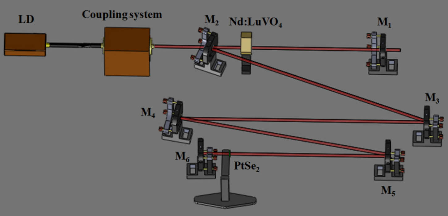
Figure 1.Schematic diagram of the mode-locked laser using film as the saturable absorber.
3. RESULTS AND DISCUSSION
The XRD pattern of the film is presented in Fig. 2(a), showing a strong diffraction peak located at 16.82°, which corresponds to the (001) planes arranged in the direction perpendicular to the axis of , indicating layer structure of the as-prepared . Besides, three more weak diffraction peaks located at 27.76°, 32.76°, and 49.24° are detected and shown in the inset of Fig. 2(a), which are indexed to (100), (101), and (110) planes of , respectively [33]. Figure 2(b) shows the Raman spectrum of film. Three prominent peaks are identified at , , and , corresponding to , , and vibration modes, respectively. The mode is an in-plane vibration mode of platinum and selenium atoms, while the and modes are out-plane vibration modes of selenium atoms [11]. These strong characteristic Raman peaks indicate that the prepared film has good crystallinity, agreeing well with the XRD result. Figure 2(b) inset is a Raman mapping image of the peak intensity of film obtained within an area of . It shows the continuous and homogeneous signal of , indicating the good continuity and homogeneity of film. An atomic force microscope image of film is presented in Fig. 2(c), showing the clear border of the film. The cross-section height profile given in Fig. 2(d) shows the thickness of the film is about 24 nm.

Figure 2.(a) XRD pattern of the as-prepared film; inset, enlarged part of the original XRD pattern of the film; (b) Raman spectrum of ; inset, Raman mapping image of film obtained within an area of ; (c) AFM image of film; (d) cross-section height profile of film obtained from AFM image.
Figure 3(a) presents a photograph of the film grown on a quartz substrate with a size of , showing it is a semitransparent gray-colored film. The transmission electron microscope (TEM) images of the film with different magnifications are shown in Figs. 3(b) and 3(c), revealing that the synthesized is continuous and dense polycrystalline with a vertically standing layered structure. Its high-resolution transmission electron microscope (HRTEM) image presented in Fig. 3(d) demonstrates the layer structure, with an interlayer distance of 0.54 nm, agreeing well with the interlayer distance of (001) planes, and confirming the vertically grown mode of on the quartz substrate. Figure 3(e) is the selected area electron diffraction (SAED) pattern of film, showing four clear diffraction rings, from inside to outside, which can be readily ascribed to the (001), (100), (101), and (110) planes of , respectively. The detected four groups of planes agree well with the above XRD results. Figure 3(f) shows the EDS spectrum of the film, demonstrating the film is composed of two elements, platinum and selenium, with no impurity.
Figure 3.(a) Photograph of film on quartz substrate with a size of . (b), (c) TEM images of film with different magnifications; (d) HRTEM image of the film; (e) SAED pattern; (f) EDS spectrum of the film.
A pulsed laser with a pulse width of 25 ps working at 1.06 μm was used to investigate the nonlinear optical properties of the film. The relationship between the transmission and the input pulse fluence is shown in Fig. 4(a). The modulation depth () and saturation fluence () are determined to be 12.6% and , respectively. The as-prepared film was used as a saturable absorber in an laser system. The mode-locked pulse trains were recorded by a fast photodiode connected to a digital oscilloscope (Agilent DSO7104B) and are shown in different time scales in Figs. 4(b)–4(d). The pulse trains recorded on the oscilloscope show uniform intensity. The measured repetition rate is 61.3 MHz, with a pulse-to-pulse interval of 16.3 ns, corresponding to the cavity round-trip time, indicating the laser is under mode-locking operation. Much work has been done by using Group-6 TMDs, including , , , , etc. as saturable absorbers for generating pulsed lasers [34,35]. However, most of the laser mode-locking demonstrations are based on fiber lasers, while for solid-state lasers, the realization of mode-locked operation based on TMDs is rarely reported. However, as is well known, a crystal laser can be a better gain medium for high-pulse energy generation due to its large mode volume for energy storage. Currently, -switched microsecond or nanosecond lasers are usually obtained in solid-state lasers based on TMDs [36–39]. In this work, it is exciting to report the realization of solid-state mode-locked laser using as the saturable absorber.
Figure 4.(a) Nonlinear optical transmittance curve of the film; (b)–(d) typical mode-locked pulse trains recorded on different time scales of the mode-locked solid-state laser using film as a saturable absorber.
Figures 5(a) and 5(b) show the output laser spectra measured before and after mode locking, respectively, using an optical spectrum analyzer with a wavelength resolution of 0.01 nm. Their central wavelengths are 1066.572 and 1066.573 nm, respectively, nearly the same. The 3 dB bandwidth of the spectrum before mode locking is 0.035 nm, while it is 0.106 nm for the one after mode locking. The transform limited pulse width of the mode-locked laser was calculated to be 15.8 ps using the formula where denotes the pulse width of the mode-locked laser, represents the wavelength bandwidth of the mode-locked laser, is the central wavelength of the laser, is the speed of light, and 0.441 is the transform limited time-bandwidth value of a Gaussian shape pulse. Figure 5(c) is the curve of the average output power with respect to the incident pump power. The stable mode-locked operation was observed at an incident pump power of 2.23 W. The maximum average output power of the mode-locked laser can reach 180 mW at an incident pump power of 3.64 W. The calculated pulse energy is 2.94 nJ.
Figure 5.(a), (b) Output spectra of the solid state before and after mode locking, respectively; (c) average output power versus incident pump power.
4. CONCLUSIONS
In summary, we believe this is the first report of the successful generation of a stable mode-locked pulsed laser by using the novel layered as a saturable absorber. The XRD pattern and Raman spectrum indicate the layered structure and good crystallinity of film prepared by the magnetron sputtering method. The HRTEM image clearly presents its vertically grown mode on the quartz substrate. The modulation depth () and saturation fluence () of film are measured to be 12.6% and , respectively. Stable and uniform pulse trains are obtained from a -based mode-locked laser, and the 3 dB bandwidth of the mode-locked laser output spectrum is measured to be 0.106 nm. The transform limited pulse width of the mode-locked laser is calculated to be 15.8 ps. The maximum average output power of the mode-locked laser is 180 mW, and the working repetition rate is 61.3 MHz. has been explored as a completely new saturable absorber for generating mode-locked lasers in this research.
Acknowledgment
Acknowledgment. J. B. Li thanks Guangdong University of Technology for the research funds from the One-Hundred Talents Program.
References
[1] C. Y. Tang, P. K. Cheng, L. L. Tao, H. Long, L. H. Zeng, Q. Wen, Y. H. Tsang. Passively Q-switched Nd:YVO4 laser using WS2 saturable absorber fabricated by radio frequency magnetron sputtering deposition. J. Lightwave Technol., 35, 4120-4124(2017).
[2] X. Yin, Z. Ye, D. A. Chenet, Y. Ye, K. O’Brien, J. C. Hone, X. Zhang. Edge nonlinear optics on a MoS2 atomic monolayer. Science, 344, 488-490(2014).
[3] P. Wang, S. Liu, W. Luo, H. Fang, F. Gong, N. Guo, Z. Chen, J. Zou, Y. Huang, X. Zhou, J. Wang, X. Chen, W. Lu, F. Xiu, W. Hu. Arrayed van der Waals broadband detectors for dual-band detection. Adv. Mater., 29, 1-8(2017).
[4] C. Xie, C. Mak, X. Tao, F. Yan. Photodetectors based on two-dimensional layered materials beyond graphene. Adv. Funct. Mater., 27, 1-41(2017).
[5] J. Chu, F. Wang, L. Yin, L. Lei, C. Yan, F. Wang, Y. Wen, Z. Wang, C. Jiang, L. Feng, J. Xiong, Y. Li, J. He. High-performance ultraviolet photodetector based on a few-layered 2D NiPS3 nanosheet. Adv. Funct. Mater., 27, 1701342(2017).
[6] X. Chia, A. Adriano, P. Lazar, Z. Sofer, J. Luxa, M. Pumera. Layered platinum dichalcogenides (PtS2, PtSe2, and PtTe2) electrocatalysis: monotonic dependence on the chalcogen size. Adv. Funct. Mater., 26, 4306-4318(2016).
[7] M. Zhang, C. Richard, T. Howe, R. I. Woodward, E. J. R. Kelleher, F. Torrisi, G. Hu, S. V. Popov, J. R. Taylor, T. Hasan. Solution processed MoS2-PVA composite for sub-bandgap mode-locking of a wideband tunable ultrafast Er:fiber laser. Nano Res., 8, 1522-1534(2015).
[8] K. C. Kwon, S. Choi, K. Hong, C. W. Moon, Y. S. Shim, D. H. Kim, T. Kim, W. Sohn, J. Jeon, C. H. Lee, K. T. Nam, S. Han, S. Y. Kim, H. W. Jang. Wafer-scale transferable molybdenum disulfide thin-film catalysts for photoelectrochemical hydrogen production. Energy Environ. Sci., 9, 2240-2248(2016).
[9] Y. Wang, L. Li, W. Yao, S. Song, J. T. Sun, J. Pan, X. Ren, C. Li, E. Okunishi, Y. Wang, E. Wang, Y. Shao, Y. Y. Zhang, H. Yang, E. F. Schwier, H. Iwasawa, K. Shimada, M. Taniguchi, Z. Cheng, S. Zhou, S. Du, S. J. Pennycook, S. T. Pantelides, H. Gao. Monolayer PtSe2, a new semiconducting transition-metal-dichalcogenide, epitaxially grown by direct selenization of Pt. Nano Lett., 15, 4013-4018(2015).
[10] M. Yan, E. Wang, X. Zhou, G. Zhang, H. Zhang, K. Zhang, W. Yao, N. Lu, S. Yang, S. Wu. High quality atomically thin PtSe2 films grown by molecular beam epitaxy. 2D Mater., 4, 045015(2017).
[11] Y. Zhao, J. Qiao, Z. Yu, P. Yu, K. Xu, S. Lau, W. Zhou, Z. Liu, X. Wang, W. Ji, Y. Chai. High-electron-mobility and air-stable 2D layered PtSe2 FETs. Adv. Mater., 29, 1604230(2017).
[12] Z. Wang, Q. Li, F. Besenbacher, M. Dong. Facile synthesis of single crystal PtSe2 nanosheets for nanoscale electronics. Adv. Mater., 28, 10224-10229(2016).
[13] C. Yim, K. Lee, N. McEvoy, M. O’Brien, S. Riazimehr, N. C. Berner, C. P. Cullen, J. Kotakoski, J. C. Meyer, M. C. Lemme, G. S. Duesberg. High-performance hybrid electronic devices from layered PtSe2 films grown at low temperature. ACS Nano, 10, 9550-9558(2016).
[14] L. H. Zeng, S. H. Lin, Z. J. Li, Z. X. Zhang, T. F. Zhang, C. Xie, C. H. Mak, Y. Chai, S. P. Lau, L. B. Luo, Y. H. Tsang. Fast, self-driven, air-stable and broadband photodetector based on vertically aligned PtSe2/GaAs heterojunction. Adv. Funct. Mater., 28, 1705970(2018).
[15] K. Ullah, S. Ye, Z. Lei, K. Y. Cho, W. C. Oh. Synergistic effect of PtSe2 and graphene sheets supported by TiO2 as cocatalysts synthesized via microwave techniques for improved photocatalytic activity. Catal. Sci. Technol., 5, 184-198(2015).
[16] M. Gong, H. Yu, X. Wushouer, P. Yan. Passively mode-locked Nd:YVO4 picosecond laser with oblique incidence on SESAM. Laser Phys. Lett., 5, 514-517(2008).
[17] C. Y. Tang, Y. Chai, H. Long, L. L. Tao, L. H. Zeng, Y. H. Tsang, L. Zhang, X. C. Lin. High-power passively mode-locked Nd:YVO4 laser using SWCNT saturable absorber fabricated by dip coating method. Opt. Express, 23, 4880-4886(2015).
[18] Z. Sun, T. Hasan, F. Torrisi, D. Popa, G. Privitera, F. Q. Wang, F. Bonaccorso, D. M. Basko, A. C. Ferrari. Graphene mode-locked ultrafast laser. ACS Nano, 4, 803-810(2010).
[19] P. L. Huang, S. C. Lin, C. Y. Yeh, H. H. Kuo, S. H. Huang, G. R. Lin, L. J. Li, C. Y. Su, W. H. Cheng. Stable mode-locked fiber laser based on CVD fabricated graphene saturable absorber. Opt. Express, 20, 2460-2465(2012).
[20] J. L. Xu, X. L. Li, Y. Z. Wu, X. P. Hao, J. L. He, K. J. Yang. Graphene saturable absorber mirror for ultra-fast-pulse solid-state laser. Opt. Lett., 36, 1948-1950(2011).
[21] S. Liu, Z. Li, Y. Ge, H. Wang, R. Le, X. Jiang, J. Li, Q. Wen, H. Zhang. Graphene/phosphorene nano-heterojunction: facile synthesis, nonlinear optics and ultrafast photonics applications with enhanced performance. Photon. Res., 5, 662-668(2017).
[22] Z. Luo, D. Wu, B. Xu, H. Xu, Z. Cai, J. Peng, J. Weng, S. Xu, C. Zhu, F. Wang, Z. Sun, H. Zhang. Two-dimensional material-based saturable absorbers: towards compact visible-wavelength all-fiber pulsed lasers. Nanoscale, 8, 1066-1072(2016).
[23] K. Wu, X. Zhang, J. Wang, X. Li, J. Chen. WS2 as a saturable absorber for ultrafast photonic applications of mode-locked and Q-switched lasers. Opt. Express, 23, 11453-11461(2015).
[24] C. Zhao, Y. Zou, Y. Chen, Z. Wang, S. Lu, H. Zhang, S. Wen, D. Tang. Wavelength-tunable picoseconds soliton fiber laser with topological insulator: Bi2Se3 as a mode locker. Opt. Express, 20, 27888-27895(2012).
[25] C. Zhao, H. Zhang, X. Qi, Y. Chen, Z. Wang, S. Wen, D. Tang. Ultra-short pulse generation by a topological insulator based saturable absorber. Appl. Phys. Lett., 101, 106101(2012).
[26] Y. Chen, G. Jiang, S. Chen, Z. Guo, X. Yu, C. Zhao, H. Zhang, Q. Bao, S. Wen, D. Tang, D. Fan. Mechanically exfoliated black phosphorus as a new saturable absorber for both Q-switching and mode-locking laser operation. Opt. Express, 23, 12823-12833(2015).
[27] X. Su, Y. Wang, B. Zhang, R. Zhao, K. Yang, J. He, Q. Gu, Z. Jia, X. Tao. Femtosecond solid-state laser based on a few-layered black phosphorus saturable absorber. Opt. Lett., 41, 1945-1948(2016).
[28] B. Zhang, F. Lou, R. Zhao, J. He, J. Li, X. Su, J. Ning, K. Yang. Exfoliated layers of black phosphorus as saturable absorber for ultrafast solid-state laser. Opt. Lett., 40, 3691-3694(2015).
[29] L. Kong, Z. Qin, G. Xie, Z. Guo, H. Zhang, P. Yuan, L. Qian. Black phosphorus as broadband saturable absorber for pulsed lasers from 1 μm to 2.7 μm wavelength. Laser Phys. Lett., 13, 045801(2016).
[30] Y. Song, S. Chen, Q. Zhang, L. Li, L. Zhao, H. Zhang, D. Tang. Vector soliton fiber laser passively mode locked by few layer black phosphorus-based optical saturable absorber. Opt. Express, 24, 25933-25942(2016).
[31] X. Jiang, S. Liu, W. Liang, S. Luo, Z. He, Y. Ge, H. Wang, R. Cao, F. Zhang, Q. Wen, J. Li, Q. Bao, D. Fan, H. Zhang. Broadband nonlinear photonics in few-layer MXene Ti3C2Tx(T = F, O, or OH) nanosheets. Laser Photon. Rev., 12, 1700229(2017).
[32] F. Torrisi, D. Popa, S. Milana, Z. Jiang, T. Hasan, E. Lidorikis, A. C. Ferrari. Stable, surfactant-free graphene-styrene methymethacrylate composite for ultrafast lasers. Adv. Opt. Mater., 4, 1088-1097(2016).
[33] L. Li, W. Wang, Y. Chai, H. Li, M. Tian, T. Zhai. Few-layered PtS2 phototransistor on h-BN with high gain. Adv. Funct. Mater., 27, 1701011(2017).
[34] J. Du, Q. Wang, G. Jiang, C. Xu, C. Zhao, Y. Xiang, Y. Chen, S. Wen, H. Zhang. Ytterbium-doped fiber laser passively mode locked by few-layer molybdenum disulfide (MoS2) saturable absorber functioned with evanescent field interaction. Sci. Rep., 4, 6346(2014).
[35] H. Xia, H. P. Li, C. Y. Lan, X. X. Zhang, S. J. Zhang, Y. Liu. Ultrafast erbium-doped fibre laser mode-locked by a CVD-grown molybdenum disulfide (MoS2) saturable absorber. Opt. Express, 22, 17341-17348(2014).
[36] Y. Sun, Y. Bai, D. Li, L. Hou, B. Bai, Y. Gong, L. Yu, J. Bai. 946 nm Nd:YAG double Q-switched laser based on monolayer WSe2 saturable absorber. Opt. Express, 25, 21037-21048(2017).
[37] W. J. Tang, Y. G. Wang, K. J. Yang, J. Zhao, S. Z. Zhao, G. Q. Li, D. C. Li, T. Li, W. C. Qiao. 1.36 W passively Q-switched YVO4/Nd:YVO4 laser with a WS2 saturable absorber. IEEE Photon. Technol. Lett., 29, 470-473(2017).
[38] B. Xu, Y. Cheng, Y. Wang, Y. Huang, J. Peng, Z. Luo, H. Xu, Z. Cai, J. Weng, R. Moncorge. Passively Q-switched Nd:YAlO3 nanosecond laser using MoS2 as saturable absorber. Opt. Express, 22, 28934-28940(2014).
[39] F. Jia, H. Chen, P. Liu, Y. Huang, Z. Luo. Nanosecond-pulsed, dual-wavelength passively Q-switched c-cut Nd:YVO4 laser using a few-layer Bi2Se3 saturable absorber. IEEE J. Sel. Top. Quantum Electron., 21, 1601806(2015).


