Unlike organic–inorganic hybrid perovskites, all-inorganic cesium lead halide perovskites hold great promise for developing high-performance optoelectronic devices, owing to their improved stability. Herein, we investigate the perovskite-related CsPb2Br5 nanoplatelets (NPLs) with tunable emission wavelengths via changing the reaction temperatures to 100°C, 120°C, and 140°C. Reaction temperature plays a key role in determining the shapes and thicknesses of the resulting CsPb2Br5 NPLs. A higher temperature is in favor of the formation of smaller and thicker NPLs. To develop their potential applications in optoelectronic devices, green light emitting diodes (LEDs) and photodetectors based on CsPb2Br5 NPLs are fabricated. The green LEDs based on CsPb2Br5 NPLs synthesized at 140°C exhibit an excellent pure green emission (full width at half-maximum of <20 nm) and display a luminous efficiency of 34.49 lm/W under an operation current of 10 mA. Moreover, the photodetector based on CsPb2Br5 NPLs synthesized at 100°C has better performance with a rise time of 0.426 s, a decay time of 0.422 s, and a ratio of the current (with and without irradiation) of 364%.
Solution-processed perovskite materials have attracted wide and close attention because of their outstanding optoelectronic properties, such as high light absorption coefficients (105 cm−1), notable optical nonlinearities, long electron–hole diffusion lengths (μ), and tunable bandgaps [1–5], which exhibit promising applications in photodetectors [6–8], lasers [9,10], light-emitting diodes (LEDs) [11,12], and solar cells [13,14]. In particular, solar cells based on organic–inorganic hybrid perovskites show a conversion efficiency over 21% [15]. However, hybrid organic–inorganic perovskites suffer from poor thermal stability due to the volatile organic constituents [16], thus severely hindering their practical applications.
Recently, all-inorganic perovskites (, , Br, I) have been demonstrated as an alternative candidate because of their enhanced stability and outstanding electronic properties compared to their hybrid organic–inorganic counterparts, which have aroused many studies, including solar cells, photodetectors, LEDs, and lasers [17–20]. Interestingly, the established colloidal synthetic approaches enable precise control of shape and size of the nanocrystals. Thus, quantum dots (QDs), nanowires, and nanosheets have been demonstrated [21–23]. Meanwhile, two-dimensional (2D) perovskites with nanoplatelet (NPL) structure have attracted intense attention due to the difference in their ionic nature and excellent optoelectronic properties compared with the traditional colloidal QDs. For example, Alivisatos et al. reported the controlled growth of NPLs with lateral sizes of by adjusting the temperature [24]. Manna reported the room-temperature synthesis of NPLs with lateral dimensions below 50 nm, the thickness of which could be precisely controlled from 3 to 5 monolayers by tuning the amount of HBr [25]. NPLs reported by Alivisatos’ and Manna’s groups possessed a cubic phase. Shortly thereafter, nanosheets with an orthorhombic crystal structure and nanosheets with tetragonal phases were synthesized by Dong’s group and photodetectors based on nanosheets were fabricated with high on/off ratios [26]. 2D atomically thin nanosheets with a thicknesses of about 3.3 nm and edge lengths of about 1 μm have been used to fabricate flexible photodetectors, which exhibit photosensitivities with on/off ratios of higher than [27]. Liu and coworkers exhibited that thinner NPLs were produced from shorter chain amines by varying the hydrocarbon chain composition of carboxylic acids and amines [28].
More recently, tetragonal perovskite-related (, , Sn, , Br, I) have been demonstrated, which are obviously different from the crystal structure of perovskite. For tetragonal structure, one layer of Cs ions exists between two layers of Br–Pb [29]. Wang et al. reported that the dual-phase all-inorganic composite nanoparticles could be developed as LEDs. They claimed that nanoparticles could improve the current efficiency by decreasing diffusion length of excitons [30]. Yu et al. reported a fast anion exchange for the large-scale fabrication of highly luminescent NPLs [31]. Meanwhile, we reported on a microplates laser with superior crystallinity and enhanced stability [32]. However, to the best of our knowledge, the controlled growth of NPLs by varying the reaction temperature and their related device applications have not yet been reported to date. Thus, in comparison with perovskite, it is still challenging to modulate the emission properties of NPLs and develop their potential applications for LEDs and photodetectors.
Sign up for Photonics Research TOC. Get the latest issue of Photonics Research delivered right to you!Sign up now
In this paper, we report on highly luminescent NPLs with tunable emission wavelengths from blue (467 nm) to bright green (518 nm). By changing the temperature of the precursor solution from 100°C to 140°C, we observe that the reaction temperature plays a critical role in tuning the shapes and optical properties of NPLs. The higher temperatures are in favor of the generation of smaller and thicker NPLs, resulting in a redshift of the emission peaks. We demonstrate their potential applications in highly bright green LEDs, which achieve a peak emission wavelength of 538 nm, a full width at half-maximum (FWHM) of 18 nm, and a luminous efficiency of when operated with a driving current of 10 mA. Moreover, NPLs synthesized at different reaction temperatures are fabricated into photodetectors, and a brief comparison among them is studied. The photodetectors based on NPLs synthesized at 100°C exhibit faster response times and larger ratios than others due to NPLs with lateral sizes of more than 1 μm and good optoelectronic properties.
2. EXPERIMENTAL
The all-inorganic perovskite NPLs were prepared by a hot-injecting method through the reaction of a Cs-oleate precursor solution and precursors in 1-octadecene (ODE) under nitrogen atmosphere with a long-chain n-octylamine (OCA) and oleic acid (OA) as the surfactants. Typically, for the synthesis of NPLs, a mixture of 100 mg , 7.5 mL of ODE, 0.5 mL of OCA, and 0.5 mL of OA was loaded into a 100 mL three-necked flask used as precursors, which was degassed under nitrogen flow at 100°C for 0.5 h. After that, 0.375 mL of the Cs-oleate precursor was quickly injected into the flask by the use of a pipettor. The mixture was kept at different temperatures for about 3 h for NPL growth. For the synthesis of NPLs at 120°C and 140°C, precursors were prepared at 120°C and 140°C, respectively. For the isolation and purification of NPLs, the resulting products were precipitated using toluene and separated via centrifugation. After five centrifugations, the supernatant was discarded and the NPLs precipitate was dispersed in toluene, forming long-term stable solutions.
A blue GaN LED chip () was welded in a groove with a radius of about 2 mm. The quantity of NPLs coating the blue GaN chip plays a key role for achieving highly monochromatic green emission from the blue LED. Thus, 2 mg NPLs taken out from the resulting powder were redispersed in 5 mL toluene, and then ultrasonic treatment of approximately 10 min was carried out to disperse the NPLs sufficiently. Following, the 0.005 mL NPL solution was directly dropped into the LED groove by using a pipettor. Then, the LEDs were put onto a heater with a temperature of 60°C to promote the volatilization of toluene and to form NPL film. The thickness of the film produced by the 0.005 mL NPL solution was measured to be about 150 nm, and the film thickness has linear relationship with the quantity of the dropped solution. The emission spectrum of the green LEDs was recorded by a PR670 spectrometer.
The photodetector device was prepared by spraying the NPL toluene solution on a gold interdigital electrode based on an substrate with 10 μm space of adjacent fingers. The current–voltage (I–V) features of the photodetector were measured by changing the bias voltage from to 10 V. The photocurrent–time response of the photodetector was measured in the dark and illumination by using the blue laser of 405 nm at a fixed applied bias of 6 V. All the current results were measured with a Keithley 4200 electrometer.
The structures and optical properties of the synthesized NPLs were characterized by combined techniques. Scanning electron microscopy (SEM) images were recorded by an electron microscope (JEOL, JSM-7800F, Japan). Atomic force microscopy (AFM) imaging was carried out on a scanning probe microscope (Nanonavi, SPA-400SPM, Japan) using a tapping mode. The crystal phases of all samples were characterized by x-ray diffraction (XRD) with Cu Ka radiation (Shimadzu, XRD-6100, Japan). Absorption spectra were recorded, ranging from 400 to 600 nm, by a UV–vis–NIR spectrophotometer (Shimadzu, UV-3600, Japan). Photoluminescence (PL) spectroscopy was measured by a fluorescence spectrophotometer, which includes a Xe lamp as the excitation source with optical filters. The PL decay lifetimes and PL quantum yields (PLQYs) were characterized by Edinburgh Analytical Instruments (FLSP920) equipped with a continuous Xe-900 Xenon lamp, a uF900 microsecond flash lamp, and a 365 nm light filter. We measured the PLQY of these NPLs in toluene solutions due to their good solubility in toluene, which is often used as a solvent to measure the PLQY of perovskite materials. All tests were performed at room temperature.
3. RESULTS AND DISCUSSION
A. Characterization of CsPb2Br5 NPLs
The fast nucleation and growth dynamics of the resulting nanocrystals were determined by the ions in the complex decomposition reaction. The reactions were carried out at three different temperatures of 100°C, 120°C, and 140°C.
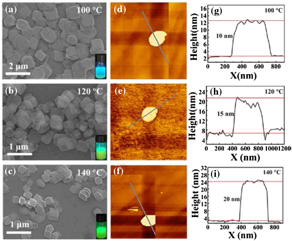
We noticed that the reaction temperature played a crucial role in regulating the sizes and thicknesses of the resulting NPLs. Morphology and thickness characterizations of were performed with SEM and AFM, as shown in Fig. 1. The SEM images show that all the prepared are of microplate or NPL shape and of highly uniform size distribution. For the 100°C reaction products, the average grain size of the microplates with blue PL emission is about 1 μm [Fig. 1(a)]. The microplates then gradually evolved to NPLs with the grain size decreasing as reaction temperature increased, as demonstrated in Figs. 1(a)–1(c). Reactions conducted at higher temperatures present redshifted phenomena. For example, at 120°C, NPLs with cyan emission and an average grain size of 500 nm were formed. At 140°C, NPLs with an average grain size of 200 nm and green PL emission were observed. From the AFM topography images [Figs. 1(d)–1(f)] and line profiles [Figs. 1(g)–1(i)], the thicknesses of the NPLs increased from 10 to 20 nm when the reaction temperatures increased from 100°C to 140°C. A conclusion could be drawn that a lower temperature facilitates the generation of larger and thinner NPLs and a higher temperature facilitates the generation of smaller and thicker NPLs. A similar phenomenon was also observed in NPLs previously [24].
Figure 1.Study of the influence of reaction temperature on NPLs. (a)–(c) SEM images, (d)–(f) AFM topography images, and (g)–(i) line profiles of layers.
The morphologies and compositions of the NPLs synthesized at 140°C were further confirmed by transmission electron microscope (TEM) and energy-dispersive spectroscopy (EDS) analyses, as shown in Fig. 2. The high-resolution TEM (HRTEM) image of the NPLs [Fig. 2(b)] reveals that the interfringe distance is about 0.3 nm, corresponding to the (220) lattice plane of the crystal. A typical single NPL synthesized at 140°C was used for EDS and mapping image analysis to confirm the uniform distribution of the Cs, Pb, and Br components [Figs. 2(c)–2(g)]. The molar ratio of Cs/Pb/Br is , perfectly matching with the stoichiometry of the compound.
Figure 2.Morphology and EDS of an individual NPL synthesized at 140°C. (a) TEM image and (b) HRTEM image. (c)–(f) Element mapping and (g) EDS spectrum.
Further details of NPLs were revealed by XRD, PL emission spectra, the UV–vis absorption spectra, and PL decay curves. As shown in Fig. 3(a), the diffraction peaks are strong and sharp, which indicate that the obtained NPLs are highly crystalline. The diffraction peaks centered at 11.8°, 23.4°, 29.4°, 35.6°, and 48° correspond to the (002), (210), (213), (312), and (413) crystal planes, respectively, which match well with the pure tetragonal perovskite-related phase (PDF#25-0211) [33]. It can be seen that the XRD pattern of is totally different from that of [19–21], resulting from their distinct crystal structures. For , one layer of ion is sandwiched between two layers of , which is distinct from the crystal structure of with a three-dimensional connected structure, as shown in Fig. 3(b).
Figure 3.(a) XRD pattern. (b) Crystal structures of and . (c) PL and UV–vis absorption spectra. (d) PL decay traces of NPLs.
The UV–vis absorption and PL properties of NPLs synthesized at different temperatures are presented in Fig. 3(c). Sharp exciton peaks play a dominant role in the absorption spectrum, which are similar to optical features previously reported for nanocrystals [34]. The absorption and emission peaks present progressive redshifts and Stokes shifts () with increasing temperature. Reactions at higher temperatures made the PL emission peaks shift continuously to longer wavelengths, from blue (467 nm) to green (518 nm) [Fig. 3(c)]. The redshift could be understood by the quantum size effect and is further confirmed by increasing thickness at higher temperature [24,28]. The PL emission spectrum of the NPLs synthesized at 140°C [Fig. 3(c)] shows a symmetric spectrum peaked at 518 nm with an FWHM of 18 nm, indicating its potential application as green phosphor for pure green LEDs.
To further understand the decay dynamics of NPLs, the time-resolved PL decay curves of NPLs synthesized at different temperatures are presented in Fig. 3(d). The PL decay of the NPLs can be fitted by a second-order exponential function: where and represent the decay time of the PL emission, and and are the amplitudes of the decay parts. The average lifetime can be obtained by the fitting parameters according to the following formula:
From Table 1, we can observe that the radiative recombination lifetime () decreases from 5.2 to 4.2 ns and the nonradiative recombination lifetime () increases from 9.2 to 32.9 ns with increasing reaction temperature. Through Eq. (2) and the fitting parameters, the average lifetimes of NPLs synthesized at 100°C, 120°C, and 140°C are 5.9, 6.5, and 9.7 ns, respectively. The lifetimes of green NPLs synthesized at 140°C are significantly longer than those of green QDs, indicating higher ratios of exciton recombination and fewer transitions at defect states [35]. According to previous reports, a shorter radiative recombination lifetime () can result in a higher PLQY [36]. For example, is more than eight times smaller than for the green NPLs, which results in its highest PLQY (63%).
Temp (°C)
τ1 (ns)
τ2 (ns)
τave (ns)
PLQY (%)
100
5.2
9.2
5.9
11
120
4.8
16.3
6.5
24
140
4.2
32.9
9.7
63
Table 1. Lifetimes and PLQYs of NPLs Synthesized at Different Temperatures
B. Optoelectronic Properties of the Fabricated Green LEDs
As mentioned above, NPLs synthesized at 140°C are capable of emitting narrow-band green light, which inspired us to develop their potential applications in green LEDs as green phosphor. Green LEDs were fabricated by drop-casting the NPL solution onto LED chips. Blue LEDs with an emitting wavelength of 450 nm were used as the excitation source. To analyze the suitable quantity of NPLs for highly monochromatic green light emission, the emission spectra of the as-coated LEDs were recorded by the PR670 spectrometer.
Figure 4(a) presents the schematic of the coated LEDs. As the amount of NPLs increase, the variation of the emission spectra at a fixed driving current of 10 mA is presented in Fig. 4(b). Two emission peaks located at 450 and 538 nm could be observed, which belong to the emission of the blue GaN chip and the green NPLs, respectively. With increasing the quantity of the NPL solution, the intensity of blue emission peaked at 450 nm, decreased slowly, and nearly vanished when the blue emission was absorbed entirely by the thick NPL layer. The green emission intensity increased obviously, but it achieved a maximum while the deposition volume was 0.015 mL, and then decreased even the NPL solution further increased. Therefore, the thickness of the NPL layer has an obvious influence on the intensities of blue light and green light. Figure 4(c) shows the variation of the Commission Internationale Ed I’eclairage (CIE) chromaticity coordinates with changing emission spectra from pure blue to green, along with the increasing quantity of NPL solution. It could be observed that the coordinates reached the green region when the quantity of the NPL solution is 0.015 mL. The coordinate (0.190, 0.404) corresponds to the deposition volume of 0.015 mL, which is taken as the first point. Finally, the chromaticity coordinates of the green LEDs reach (0.250, 0.690) when the NPL solution deposition volume is 0.050 mL.
Figure 4.(a) Schematic of LEDs coated with NPLs. (b) Emission spectra and (c) chromaticity coordinate variations of LEDs coated with different amount of NPLs. (d) Emission spectra and (e) chromaticity coordinates of coated LEDs under different driving currents. The inset shows photographs of coated LEDs without and with injection current.
Figure 4(d) shows the emission spectra of the LEDs operated under different currents of 5, 50, 100, 150, and 200 mA. Along with the increasing current, the spectra intensity increases gradually with no obvious shift, which indicates a relative thermal stability. CIE chromaticity coordinates of these emission spectra are given in Fig. 4(e). The chromaticity coordinates are overlapped while the driving current reached 200 mA, further confirming that these emission spectra have no shift. The inset in Fig. 4(d) presents photographs of the green LEDs without/with injection currents. It is clearly observed that pure green light emission is coupled out of LEDs coated with NPLs.
Meanwhile, it is worth noting that along with the addition of NPLs, the green emission (around 538 nm) has a redshift. Also, compared with the PL emission in the solution shown in Fig. 3(c), the green emission peak has a redshift. It was speculated that both of these redshifts might be induced for the same reason: NPL particle aggregation in the solid state. According to spectral overlap of NPLs synthesized at 140°C between absorption and emission spectra shown in Fig. 3(c), the absorption intensity of the wavelength overlapping the short wavelength of emission was larger than that overlapping the long one, which resulted in stronger self-absorption in the short wavelength. This kind of spectral overlap generally can be described in terms of Förster distance (), and redshift induced by the reabsorption that always occurs in small interparticle distances less than [37,38]. In our case, NPLs would aggregate together after toluene volatilized. Therefore, the short wavelengths (490–518 nm) of the emission were weakened, and as a consequence, the long wavelengths of the emission were comparatively strengthened. Along with the addition of NPLs, the number of aggregated NPLs increased, resulting in the continual redshift shown in Fig. 4(b).
Figure 5(a) shows the current–voltage (I–V) characteristics of the bare blue LEDs and coated green LEDs. It can be seen that the voltage-current curve of the coated LEDs is nearly consistent with the one of the bare LEDs, which indicates that the direct coating of NPLs will not worsen the electrical performance of the fabricated green LEDs. As shown in Fig. 5(b), there is no remarkable fluctuation of the emission peak only in between 530 and 531 nm in the wide current range from 1 to 200 mA, verifying that no shift of the PL spectrum occurred. Along with the increase of the driving current, the unobvious variation range of the FWHM is from 18 to 20 nm, which presented an increasing tendency. This phenomenon could be ascribed to the heat generation induced by the increasing injection current. A variety of light-emitting mechanisms were involved in the spectral line broadening, and the dominating contribution to that was the exciton–acoustic-phonon coupling [39–41].
Figure 5.(a) I–V curve of bare LEDs and coated LEDs. (b) Variation of FWHM and emission peak of coated LEDs under different injection currents. Luminous flux and luminous efficiency of (c) bare LEDs and (d) coated LEDs.
The luminous performance of the fabricated green LEDs was tested with increasing driving currents from 10 to 200 mA. In order to make a comparison, the luminous performance of the bare blue LEDs was also evaluated. As presented in Figs. 5(c) and 5(d), respectively, both bare LEDs and coated LEDs have the same change trend: luminous flux increases but the luminous efficiency decreases while increasing the driving current. The luminous efficiency of the green LEDs decreases from under 10 mA driving current to . The luminous efficiency of the blue LEDs also has an obvious decrease from at 10 mA to at 200 mA, which is one factor leading to the decreasing luminous efficiency of green LEDs.
C. Performance of the Photodetectors Based on CsPb2Br5 NPLs
The photodetector device was prepared by dropping a 20 μL NPL solution synthesized at different temperatures on a gold interdigital electrode based on an substrate with the adjacent finger widths of 10 μm. The device structures and surface SEM topographies of the NPL photodetectors are illustrated in Figs. 6(a)–6(c). As shown in Fig. 6(c), most of the as-prepared NPLs were successfully attached between two gold electrodes.
Figure 6.(a) Schematic diagram of the fabricated photodetector device. (b) SEM image and (c) magnified SEM image of the device. (d) Band profile of the NPL photodetector. (e)–(g) Current–voltage (I–V) characteristics of NPL photodetectors without and with incident light of 405 nm by changing the bias voltage from to 10 V.
The measured current–voltage (I–V) curves of the devices with NPLs synthesized at different reaction temperatures are shown in Figs. 6(e)–6(g), respectively. Clearly, the I–V curves present as nonlinear with increasing bias, indicating Schottky contact between NPLs and gold electrodes. As presented in Fig. 6(d), the mismatch between the work function of the gold electrode (5.1 eV) and the energy levels of the NPL materials leads to the Schottky contact [42,43]. Meantime, the small energy barrier between the gold electrode and NPLs is favorable for the collection of the carrier under the applied voltage, which can be used to further improve the photodetecting performances.
The photocurrent–time response of the photodetector was measured in the dark and under illumination by using the blue laser at a fixed bias of 6 V, as presented in Fig. 7. The results indicate that all these NPL photodetectors have highly stable photoresponses. The output current increases significantly under illumination. For example, the photocurrent and dark current of NPLs synthesized at 100°C photodetectors are 650 and 140 nA under 6 V bias, as shown in Fig. 7(a). It could be obviously found that the ratio of the current (with and without irradiation) could achieve as large as 364%, which is significantly higher than 179% and 59% of NPLs synthesized at the 120°C and 140°C photodetectors, as shown in Table 2, indicating that the photodetectors based on NPLs synthesized at 100°C have high-quality photosensitive switches. The responsivities of the photodetectors based on NPLs synthesized at 100°C, 120°C, and 140°C are 340, 74, and μ, respectively. In Figs. 6(b), 6(d), and 6(f), we analyze the response times of these NPL photodetectors. The rise and decay times of the NPLs synthesized at the 100°C photodetector are 0.426 and 0.422 s, respectively, which is faster than those of the NPLs synthesized at 120°C and 140°C. We concluded that the NPLs synthesized at the 100°C photodetector had better performance than others, in terms of ratios, responsivities, and response times, as shown in Table 2. When NPLs were directly dropped onto a gold electrode with a 10 μm space of adjacent fingers, the NPLs synthesized at 100°C attached well between two adjacent fingers, owing to the large size of more than 1 μm, which is one of the dominating factors contributing to the performance improvement. In addition, the optical bandgap of the NPLs synthesized at 100°C is narrower and it absorbs a larger portion of blue light than others [Fig. 3(c)]. Thus, the ratios and response times of the photodetectors should be improved, owing to the efficient charge separation and transport [44].
Figure 7.(a), (c), and (e) Current–time (I–T) curves of the photodetectors. (b), (d), and (f) Rise times and the decay times of the photodetectors with incident light of 405 nm at the bias of 6 V.
In summary, a series of emission-wavelength-tunable NPLs have been prepared using a hot-injecting method by changing the reaction temperature. The emission peaks presented obviously redshift from blue to bright green with increasing reaction temperature from 100°C to 140°C. Furthermore, the green LEDs based on NPLs synthesized at 140°C and the photodetectors based on NPLs synthesized at 100°C exhibit excellent performance. We believe that the emission-wavelength-tunable NPLs with excellent optoelectronic properties can be widely used in the fields of photodetectors, LEDs, and photovoltaics.
[40] J. Li, X. Yuan, P. Jing, J. Li, M. Wei, J. Hua, J. Zhao, L. Tian. Temperature-dependent photoluminescence of inorganic perovskite nanocrystal films. RSC Adv., 6, 78311-78316(2016).