
Boyang Nan, Ruijin Hong, Chunxian Tao, Qi Wang, Hui Lin, Zhaoxia Han, Dawei Zhang. Thickness dependency of nonlinear optical properties in ITO/Sn composite films[J]. Chinese Optics Letters, 2023, 21(8): 081902
- Chinese Optics Letters
- Vol. 21, Issue 8, 081902 (2023)
Abstract
Keywords
1. Introduction
In recent years, nonlinear optics has attracted the interest of many researchers because of its promising applications in optoelectronics[1], optical information storage[2], all-optical devices[3], and biomedicine[4]. A permanent goal of nonlinear optics is the development of materials and devices that significantly change the refractive index using low power optical fields. However, even under strong coherent light illumination, some materials still exhibit weak optical nonlinearities and are difficult to control. This weak optical nonlinearity severely limits the nonlinear occurrences of the device, such as frequency comb generation, frequency conversion, and entangled photon generation. Currently, researchers have proposed and developed various schemes to obtain materials with excellent nonlinear properties, such as field strengthening in localized areas using composite constructions[5,6], plasma excitonic structures[7,8], and metamaterials[9,10]. However, these techniques have difficulty in controlling the amplitude field enhancement of the nonlinear response and are inefficient. Therefore, the imperative to obtain nonlinear optical (NLO) devices is to find special components that have strong stabilization and huge NLO responses.
Studies have noted that semiconductor materials, such as indium tin oxide (ITO) films, exhibit tremendous NLO properties[11,12] and have been in a special status in the area of nonlinear optics research[13]. ITO films have a unique broad bandgap and exhibit very strong NLO properties under both inter-band and intra-band excitation conditions[14,15], especially at wavelengths where the real part of the dielectric constant is close to zero (ENZ)[16,17]. The ITO film in this state not only has a large NLO response, but also provides many advantages such as its low loss performance, superior tunability, and compatibility with current optical platforms[18,19]. This specific nonlinear property makes ITO a useful substrate to enhance the nonlinear properties of other materials[20,21]. Recent studies have shown that gold nanoparticles with different particle densities on ITO substrates are induced by coherent light to produce second harmonics[22]. Wu et al. inserted an ultrathin silver layer between two ITO films to form a sandwich structure and observed large NLO enhancement[23]. In addition, simple preparation of ITO-Au nanocomposite arrays by a self-assembled nanosphere lithography (NSL) technique as well as under annealing conditions also exhibited significant two-photon absorption (TPA) saturation effects[24]. They closely coupled metallic elements with semiconductor devices, and the plasmonic excitation of the metal itself creates a massive electromagnetic field within the nanostructure body[25], which extremely facilitates light–matter interaction to improve the NLO response. Such metal–semiconductor nanostructures have high optical nonlinearity and ultrafast time responses with performance far beyond that of individual materials[26,27]. To the best of our knowledge, NLO effects have not been reported for ITO/Sn nanocomposites.
In this study, ITO/Sn composite films with a thickness of 100 nm were prepared using the electron beam (EB) thermal evaporation technique by adjusting the relative thickness ratio of the two materials, ITO and Sn. We characterized this NLO response for ITO, Sn, and ITO/Sn composite films using a typical Z-scan technique. In addition, the crystal structure, surface morphology, absorption spectra, transmission spectra, and simulated electric field distribution of the films were analyzed. Evolution of defects and changes in optical performance within the ITO/Sn composite film were demonstrated by finite-difference in temporal domain (FDTD) simulations.
Sign up for Chinese Optics Letters TOC. Get the latest issue of Chinese Optics Letters delivered right to you!Sign up now
2. Materials and Methods
Prior to the deposition process, the glass substrates were cleaned sequentially with acetone, ethanol, and deionized water by ultrasonic cleaning for 20 min, and then placed in a nitrogen stream for drying. ITO films and the Sn layer were prepared by EB evaporation from ITO ceramics (99.99%) comprising 10% (mass fraction) and high purity metal Sn particles (99.99%), respectively. A base vacuum of less than was pumped inside the chamber in the deposition process. Furthermore, the baking temperature needed to be controlled at about 370°C. The thickness of all samples was kept constant at 100 nm. Here the sample thickness was observed by an in situ quartz crystal microbalance located in an evaporation chamber. To ensure homogeneity of film thickness, all substrates were put onto a fixture of the same radius far from the shaft.
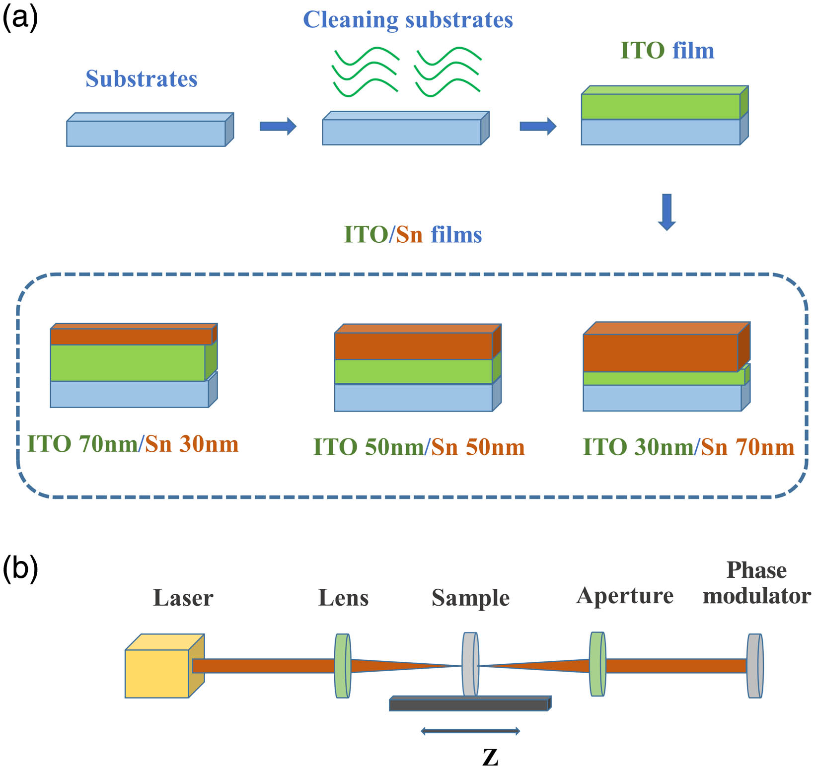
Then, the ITO film was used as a substrate, and the Sn layer was deposited on its surface. By varying their relative thicknesses, ITO/Sn composite film structures with different ratios were synthesized. In this study, the total thickness of the bilayer was controlled at a constant of 100 nm. The thickness combinations studied were ITO 70 nm/Sn 30 nm, ITO 50 nm/Sn 50 nm, and ITO 30 nm/Sn 70 nm. After the deposition process was completed, the sample was removed. For better comparison, the ITO films, Sn films, and ITO/Sn composite films in the deposited state were denoted as ITO 100 nm (S1), Sn 100 nm (S2), ITO 70 nm/Sn 30 nm (S3), ITO 50 nm/Sn 50 nm (S4), and ITO 30 nm/Sn 70 nm (S5). Figure 1(a) shows the process flow of sample preparation.
![]()
Figure 1.(a) Flow chart of sample preparation and (b) single-beam Z-scan setup.
Finally, the crystal structure of the films was acquired in phase by an X-ray diffractometer (XRD) under Cu Ka radiation () on basis of the Bruker AXS/D8 Advance system. The optical absorption coefficients and transmittance measurements were taken using a UV-Vis-NIR dual-beam spectrophotometer (Lambda 1050, PerkinElmer, USA). An atomic force microscope (AFM) (XE-100, Park System) was used to measure the surface morphology of the film and reflect the surface roughness variation of the film samples with a scanning region of . In Fig. 1(b), a single-beam Z-scan experimental setup based on optical aberration (autofocusing) is used to characterize the third-order NLO properties of the sample. The mode-locked picosecond laser with 1550 nm excitation wavelength is used as the optical excitation source with a duration of 2 ps and a repetition frequency of 100 MHz and focuses on the sample through a 15 mm lens. All measurements are conducted at room temperature.
3. Results
The X-ray diffraction spectrometers of ITO, Sn, and ITO/Sn film samples are displayed in Fig. 2. It is clear that the higher crystalline quality of the ITO film corresponds to the body centered cubic (bcc) crystal structure of (JCPDS: 06-0416)[28], and one of the strongest diffraction peaks appears near 30.45°(), corresponding to the (222) crystal plane, implying that the grains are preferentially oriented along the (222) crystal plane. The absence of characteristic peaks of Sn, SnO, or in the ITO films indicates that all tin atoms are substitutionally incorporated into the lattice. For a single tin sample, three well-defined diffraction peaks at approximately 30.7°, 32.0°, and 45.0°, corresponding to the (200), (101), and (211) planes of Sn (JCPDS card number: 04-0673), respectively, indicate the formation of metallic Sn. The diffraction peak located near 30.7°() is the sharpest, implying a selective orientation of the Sn grains towards the (200) crystal direction. Generally, for non-epi-deposition on substrates, the film favors the (222) or (200) plane[29], when the surface free energy is minimal. After adding a Sn surface layer on the ITO surface, all of the above diffraction peaks can be clearly detected, and the position of the diffraction peaks drifts slightly, which is caused by the stress generated in the film. The results show that the preparation of ITO/Sn composite film is very successful.
![]()
Figure 2.XRD plots of (a) ITO, Sn nanofilm and (b) ITO/Sn samples synthesized according to different relative thickness ratios.
Figure 3 shows typical AFM images of all samples with a scan area of . From the figure, it can be found that the apparent changes of surface morphology for the ITO/Sn composite film are strongly associated with the thickness ratio between the bilayers. The surface morphology of deposited ITO films is glossy and has the smallest root-mean-square (RMS) roughness (). For a monolayer tin sample, small and sharp nano-spherical particles with uniform particle distribution and an average diameter size of about 16.267 nm are grown on the surface, with agglomerative growth between adjacent Sn grains and an RMS roughness of approximately 4.521 nm. When a layer of Sn film is deposited on the ITO substrate, the voids between ITO grains are gradually filled with Sn grains. The relatively large grain size of Sn leads to the triggering of three-dimensional clusters during the polymerization process, which can better converge on the surface of the ITO layer and form a large number of grain boundaries. The growth of Sn on ITO surfaces is affected by many factors, such as strain energy, surface free energy, and diffusion activation energy of metal atoms with the substrate surface[30]. During the film growth process, the strain energy gradually accumulates as the thickness increases, and when the strain energy is released, the high energy at the interface will excite the film island growth[31], and the film surface will become rough, which is depicted in Figs. 3(c)–3(e). With the increase of the thickness ratio of bilayer (ITO/Sn) deposition, the morphology of the composites changes significantly: the surface becomes very rough, the RMS roughness value increases to higher values, and the particle size increases significantly and is not uniformly distributed. The increase of the Rq value is also attributed to the gain boundary between the oxide and metal layers in the composite thin film system[32]. In addition, the size of the composite film nanoparticles fluctuates with the increase of the relative thickness ratio of the bilayer film, but the overall size of the nanoparticles decreases, as shown in Fig. 3(g).
![]()
Figure 3.AFM 3D images of (a) ITO 100 nm, (b) Sn 100 nm, (c) ITO 70 nm/Sn 30 nm, (d) ITO 50 nm/Sn 50 nm, and (e) ITO 30 nm/Sn 70 nm samples. (f) RMS value change of samples and (g) average diameter of samples.
Figure 4(a) shows the optical transmission of monolayer ITO, Sn films, and ITO/Sn composite films. As can be understood from the figure, the monolayer ITO film has a large transmittance in the entire wavelength band; the transmittance grows rapidly in the UV band, and gradually reaches about 80% at Vis scope (400–800 nm) with a progressive decrease in the NIR band (800–1600 nm). Single-layer Sn films have the lowest optical transmittance due to the localized surface plasmon resonance (LSPR) properties of Sn nanoparticles. When ITO is combined with the Sn layer, the light transmittance value of the ITO/Sn composite decreases. By changing the relative thickness ratio of the bilayers, the light transmittance is found to decrease gradually. In Fig. 4(a), the ITO/Sn composite film has a reduced light transmittance rate compared to a single layer of ITO. The light absorption at the interface between ITO and Sn films reduces the light transmission rate of the ITO/Sn film. In addition, agglomeration on the ITO surface increases the scattering of incident light and thus reduces the light transmission rate.
![]()
Figure 4.Optical (a) transmittance and (b) absorption profiles of ITO, Sn, and ITO/Sn films.
The optical absorption spectrum on the prepared samples is depicted in Fig. 4(b). The deposited ITO films have very low absorption in the Vis band and gradually increasing optical absorption coefficients in the NIR band, with a very wide plasma absorption band, which is typical of ITO films. For monolayer Sn films, there is a slight surface plasmon resonance (SPR) band near 393 nm due to the LSPR effect of Sn[33]. In comparison with ITO, the absorption intensity of the ITO/Sn composite is altered across the detection band, enhancing the absorption intensity across the band. With the improvement in the relative thickness ratio between the bilayers, there is a significant shift of the weak absorption band of the sample to the left, which may be attributed to the strong coupling between ITO and Sn nanoparticles.
The single-beam Z-scan experimental system has advantages such as high sensitivity and can be used to determine the NLO characteristics of certain materials. In this experiment, third-order nonlinear absorption properties were obtained using a Z-scan-device-based system with an excitation source of . In its nonlinear state, the total absorption coefficient of the sample under strong excitation can be described as , where , , and represent the linear absorption coefficient, nonlinear absorption coefficient, and laser intensity at excitation, respectively. The normalized transmittance of all samples can be obtained using the apparatus in Fig. 1(b), and can also be obtained by[34]
The nonlinear absorption behavior of the samples was investigated at the excitation wavelength of 1550 nm, as shown in Figs. 5(a) and 5(b). The normalized Z-scan curves of samples were focused near the focal point () and showed symmetric peaks, exhibiting nonlinear saturated absorption (SA) properties. Significant normalized transmittance was observed at the point of focus for all samples (from S1 to S5) with transmittance values of 1.420, 5.783, 2.026, 7.069, and 9.801, respectively. It is clear that ITO films exhibit the weakest saturation absorption phenomenon, while monolayer Sn has excellent saturation absorption behavior due to SPR. Compared with a single layer of ITO or Sn, the ITO/Sn composites exhibit strong light transmittance at the same excitation intensity, indicating powerful light–matter interactions between the ITO-Sn composite films[36]. In Fig. 5(b), the normalized transmittance of the composite film further increases with the increase of the relative thickness of the surface Sn layer, and the peak shape broadens at the center of focus. We find that there is also fierce saturation synergistic competition mechanics between ITO and Sn layers. The ITO/Sn composite film (sample S5) exhibits the strongest SA effect when the relative thickness ratio of the bilayer film (3/7) is the smallest.
![]()
Figure 5.(a), (b) Open aperture Z-scan measurements of ITO, Sn, and ITO/Sn composite films with different relative thickness ratios.
From Fig. 5, we can see that the saturation absorption characteristics of the ITO/Sn composite film form are significantly enhanced. Among them, the ITO layer has a uniform distribution and complete and orderly surface structure, which is conducive to the better deposition of Sn particles attached to the ITO surface. This enhanced nonlinear response arises from the local field effect[37] and synergistic effect[38] between ITO and Sn nanoparticles. The local field effect promotes close contact between Sn nanoparticles and ITO, which contributes to the association between the two materials and can effectively improve the NLO properties of the composites. In addition, since ITO and Sn share the same saturable absorption properties, the synergistic effect between the two materials will also result in the enhancement of the NLO properties of the composite.
The differences in the relative size ratios in the composite films lead to different surface activities of Sn nanoparticles and compatibility between nanoparticles and ITO[39]. When the relative size ratio of the Sn layer is low, the dispersion of Sn nanoparticles on the ITO surface decreases and weakens the compatibility between ITO and Sn nanoparticles, and the synergistic effect is weakened, so the NLO properties are reduced, even lower than that of sample S2. When the proportion of Sn nanoparticles deposited on the ITO surface reaches a certain value, the compatibility between the two materials increases and the synergistic effect is greatly enhanced, so the nonlinear optics is significantly enhanced.
In Fig. 6, we provide the nonlinear absorption coefficients for ITO, Sn, and ITO/Sn composite films obtained by fitting using Z-Scan theory[40]. For nonlinear SA behavior, has a negative value. Under the same excitation conditions, the nonlinear absorption coefficients for monolayer ITO and Sn were and , respectively. When the relative thickness ratio between the bilayers was changed, the value of the composite film samples increased from to This suggests that boundary coupling between ITO and Sn films of different relative thicknesses induces the crystallinity, surface roughness, and grain size of composites, which contributes directly to variations in normalized transmittance and strong saturation absorption behavior.
![]()
Figure 6.Fitting of nonlinear absorption values (β) of monolayer ITO, Sn, and ITO/Sn composite films.
To further verify the properties of ITO/Sn composites, we simulated the electric field distribution of the samples based on FDTD analysis. We used a 1550 nm excitation light to irradiate the surface of the sample vertically and polarize it on the axis, and the simulation results are shown in Fig. 7. The ITO film has a dense and uniform surface with small roughness, showing a weak electric field intensity of 0.81. In contrast, the local electric field of monolayer Sn can reach 1.6 because it is uniformly distributed on the surface. After deposition of the synthetic ITO/Sn nanofilm, the roughness was significantly larger, the surface was irregularly distributed, and the electric field intensity of ITO/Sn composite film was significantly enhanced to 3.6. This indicates that the strong coupling between ITO and Sn films can excite a strong local electric field, resulting in an effective improvement of the optical properties of the samples. Combining simulation with experimentation can help better understand this behavior.
![]()
Figure 7.FDTD simulated electric field distributions for (a) ITO, (b) Sn, and (c) ITO/Sn films.
4. Conclusion
To summarize, we investigated the nonlinear saturation absorption behavior of ITO, Sn, and ITO/Sn composite films. The results show that the ITO/Sn composite film samples exhibit good crystallinity and optical properties. Using ITO layers as substrates can raise the nonlinear absorption behavior in the films. By adjusting the relative thickness ratio of the bilayer film, is considerably increased. It is due to this special NLO property that ITO/Sn composites will have a major role in all-optical modulation apparatuses.

Set citation alerts for the article
Please enter your email address
© Copyright 2018-2021 | Chinese Laser Press. All Rights Reserved 沪ICP备15018463号-20