Tun Cao, Yang Li, Xinyu Zhang, Yang Zou, "Theoretical study of tunable chirality from graphene integrated achiral metasurfaces," Photonics Res. 5, 441 (2017)
Copy Citation Text
Control of chirality using metamaterials plays a critical role in a diverse set of advanced photonics applications, such as polarization control, bio-sensing, and polarization-sensitive imaging devices. However, this poses a major challenge, as it primarily involves the geometrical reconfiguration of metamolecules that cannot be adjusted dynamically. Real-world applications require active tuning of the chirality, which can easily manipulate the magnitude, handedness, and spectral range of chiroptical response. Here, enabled by graphene, we theoretically reveal a tunable/switchable achiral metasurface in the near-infrared region. In the model, the achiral metasurface consists of an array of circular holes embedded through a metal/dielectric/metal trilayer incorporated with the graphene sheet, where holes occupy the sites of a rectangular lattice. Circular conversion dichroism (CCD) originates from the mutual orientation between the achiral metasurface and oblique incident wave. The achiral metasurface possesses dual-band sharp features in the CCD spectra, which are tuned over a broad bandwidth by electrically modulating the graphene’s Fermi level. By selecting aluminium as the metal materials, we numerically achieved strong CCD and considerably reduced materials costs with our nanostructures compared with the typically used noble metals such as gold and silver.
The last decade has witnessed fast development of metamaterials, an artificially structured material exhibiting electromagnetic properties not readily available in nature [1]. However, conventional metamaterials are static, that is, their electromagnetic characteristics are fixed by design, which constitutes severe limitations. Therefore, dynamic tuning of optical properties is vital for impelling metamaterials into the domain of tunable or reconfigurable devices, which has great potential to alleviate many of the complications with passive metamaterials [2,3]. To this end, a variety of tuning methods have been examined in order to change the performance of metamaterials dynamically. These include mechanical means that deform all or part of the metamaterials [4,5] and integration of sensitive materials, such as [6], yttrium-hydride [7], gallium [8], chalcogenide glass [9], and graphene [10–13], which change the fundamental material properties of the structure. Despite the great flexibility for investigating tunable metamaterials, a less reachable but significant property that fits in with external control is chirality.
Structures are chiral when they do not superpose with their mirror images [14]. Circular dichroism (CD) and optical activity known as 3D chirality have been proven highly valuable in analytical chemistry and molecular biology [15]. Meanwhile, 2D chirality linked to the effect of asymmetric transmission and circular conversion dichroism (CCD) also occurs in natural chiral molecules [16]. However, natural chiral molecules such as DNA, viruses, and amino acids usually have a weak chiroptical effect [17]. With the advance of nanotechnology, chiral metamaterials have been intensively studied [18–26]. Chiral metamaterials can improve the chiroptical response by orders of magnitude due to their strong interaction with light [27]. There is a lack of spectral tunability that allows dynamic control of the polarization of light. Tuning circular polarization can pronouncedly improve detection sensitivity when exploring the chirality of a material. It is crucial in biosensing, as biomolecules have vibration modes.
Recently, a few promising methods of achieving tunable chirality using metamaterials have been proposed. For instance, chirality can be passively switched by tilting the metamaterial against the incident beam [28] or by changing the geometry of the meta-atom [29]. Another way, which has recently attracted considerable attention, is to actively tune the response in chiral metamaterials through external stimuli, such as electric bias [30], temperature [31], or photoexcitation [32,33]. However, most chiral metamaterials integrated with active semiconductors are in the terahertz (THz) regime, and few demonstrations of the active chiral metamaterials exist at higher frequencies due to the low density of injected free electrons for semiconductors outside the THz region [34]. Lately, the concept of tunable chirality has been put forward by demonstrating that metal/chalcogenide glass/metal trilayer-based chiral metamaterials have the potential to provide a tunable optical activity in the near-infrared (NIR) region [2,35]. However, construction of such multilayer chiral metamaterials remains a challenge, especially for obtaining periodic arrays with ultrasmall chiral profiles and exact alignment in the optical region [36].
2D achiral planar metamaterials, or metasurfaces, are recognized to hold great potential for manipulating light [37]. It has been recognized that the 2D achiral planar metasurface that interacts with an incident beam can lead to pronounced chiral response indistinguishable from those seen in chiral metamaterials. Such a feature can be achieved by tilting the achiral metasurface out of its symmetry axes with respect to the incident beam. This response is termed “extrinsic chirality” due to the non-chiral nature of the structures [16]. In this case, the enantiomeric configurations, for which the CCD will be reversed, correspond to rotation around the mirror image of the axis. It offers a route for developing straightforward ultrathin polarization devices with sophisticated functionalities [38–41]. Although Singh et al. show that extrinsic chirality can be modulated in the THz region using planar achiral metamaterials [28], the relative strength of different circularly polarized waves and operating spectra cannot be tuned without tilting the metamaterials against the incident beam. Recently, a multilayer stack achiral phase-change metamaterial was proposed to actively tune the CD in the optical region [42], whereas the requirement for an ultrahigh and ultrafast laser for reversible tuning of a chiral response can be difficult. Among all the techniques for manipulating a chiroptical response, voltage control turns out to be one of the easiest ways to promote efficient operations and large-scale production. Most optical metamaterials also suffer the high cost of both Au and Ag, which thus severely hinders the practical application of these precious metals as materials for plasmonic devices [43]. Therefore, an approach for actively controlling the chiroptical effect at higher frequencies, such as the NIR region, using voltage-controlled achiral metamaterials with Al metal is desirable and necessary.
Unique electromagnetic properties of graphene sheets are paving the way toward applications in ultrathin and innovative optical devices [44]. Graphene can control its carrier mobility and conductivity by changing its electronic Fermi level via chemical or electrostatic doping [45]. This makes the continuous or structured graphene sheet a promising candidate for designing highly tunable infrared and THz metasurfaces by enabling both amplitude and phase modulation [13,46–48]. Importantly, the tuning of chiral metamaterials using graphene has been investigated in both theory [49] and experiments [50], showing that graphene-based metamaterials are gaining traction in the field of circular polarization control.
Here, we propose a new mechanism to spectrally tune the strong extrinsic 2D chiral response in the NIR regime using Al-based achiral metasurface, employed by a graphene sheet. This achiral metasurface is composed of a highly symmetric circular holes array (CHA), embedded within metal-dielectric-metal (MDM) trilayers, to create a magnetic resonance that can enhance CCD in the NIR regime. This is due mainly to the fact that the chiral response is associated with an electric and magnetic resonance dipole, and an enhancement of chirality spectroscopy demands modification of both electric (-) and magnetic (-) fields of light [51–53]. The round holes occupy the sites of a rectangular lattice to build a 2D anisotropic system, which provides two surface plasmon polariton (SPP) modes polarized along two orthogonally different lattice vectors. These two SPP polarization modes construct a chiral triad with an off-normal incident wave vector and a vector normal to the surface of CHA, hence leading to an extrinsic 2D chiroptical response once tilted around any in-plane axis that does not overlap with the array lines of mirror symmetry of the achiral metasurface.
We also demonstrate that tuning of the optical response of graphene offers a way to control the spectra of the system dynamically. Contrary to the tunable extrinsic chirality observed in previous approaches, our achiral MDM metasurface integrated with the graphene sheet enables a sharp CCD and possesses a spectral response that is sensitive to the external gate bias in the NIR region. Previous investigations were not available in the NIR, which is a highly attractive spectral region for plasmonics, for example, due to the presence of molecular vibrational fingerprints and the atmospheric transparency window [54]. Moreover, we incorporate Al instead of expensive plasmonic materials (Au or Ag) for nanostructures to obtain full compatibility with industry standard CMOS wafer-scale processing technology [43,55,56]. They are, therefore, significantly lower in complexity and cost and present tremendous potential to applications in metallic nanostructures and ultrathin active devices. It can be integrated within today’s nanophotonic systems and explores various functionalities, such as biomolecule sensing, switches, circular polarization transformers, and modulators.
2. RESULTS
A. Structure and Design
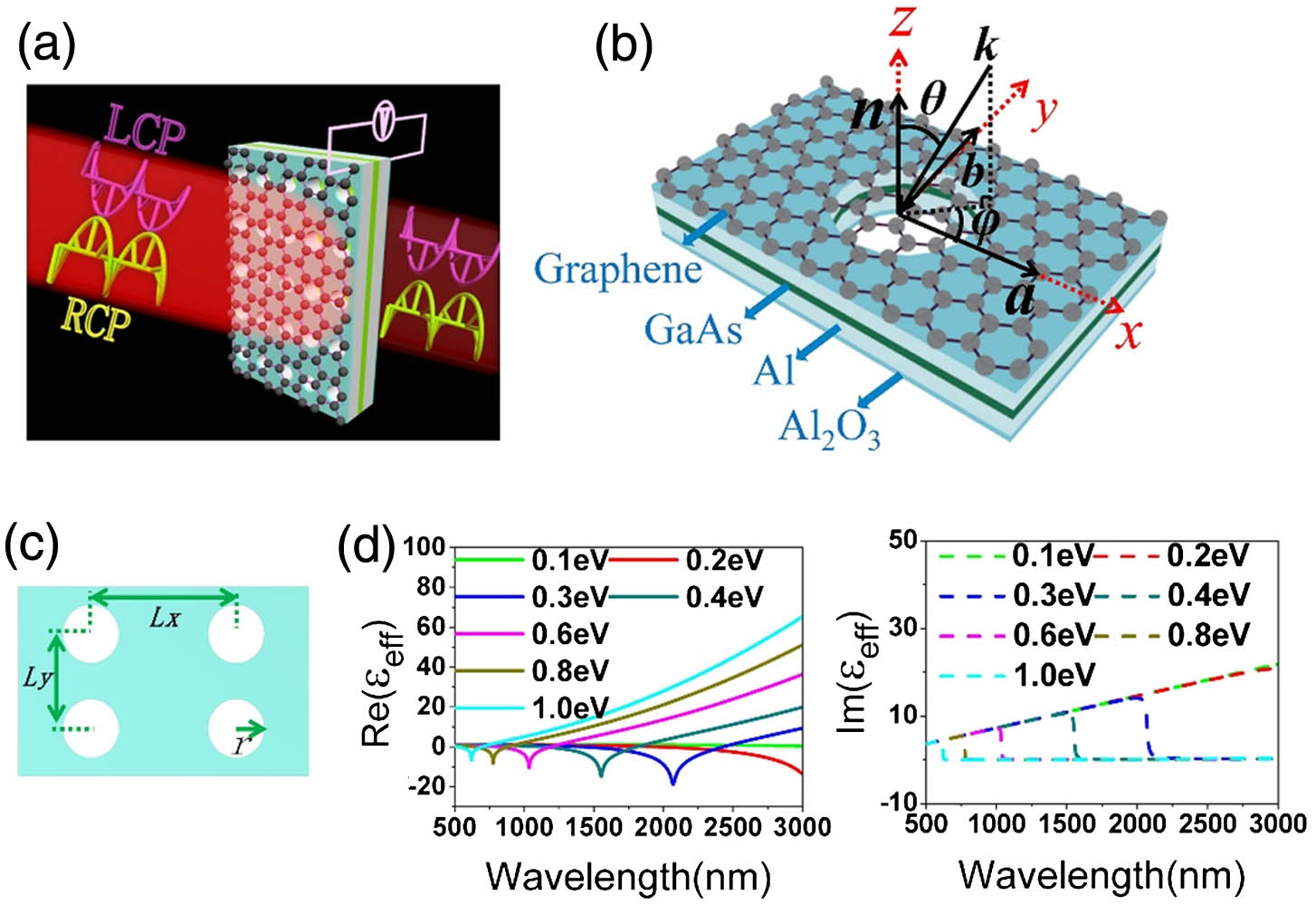
We considered an achiral metasurface composed of a rectangular lattice with pairs of round holes penetrating through two 20 nm thick Al sheets separated by a 10 nm thick dielectric (GaAs) layer. The formation of an oxide layer on Al that changes the dielectric properties of the resonator environment has been considered in the model. Here, the Al layers are assumed to form a homogeneous oxide shell with a thickness of at the expense of a shrinking Al core [56]. (Namely, the total thickness of Al layers of 20 nm is maintained in the simulation.) The dielectric constant of is defined by Malitson and Dodge [57]. In our model, a graphene layer is designed to be over the top layers [Fig. 1(a)]. In particular, the MDM multilayer forms a magnetic dipolar moment because an incident light induces a circulating AC current; the high magnetic resonance may introduce a significant variation in the transmission for left- and right-circularly polarized (LCP/RCP) waves under oblique incidences. Given that a high surface roughness of Al () is likely to have an influence on the graphene layer and its impact on the tuning of resonance, an ultrathin buffer layer, i.e., , may be introduced between the top Al () layer and graphene sheet with regard to the real fabrication [56].
Figure 1.(a) Schematic of graphene-integrated MDM-CHA. Thicknesses of the , Al, GaAs spacer, and graphene are 3, 17, 10, and 0.5 nm, respectively. (b) Illustration of the chiral triad composed of wave vector (), normal vector (), rotation angle in the plane, and different lattice vectors ( or ), marked in black. (c) Illustration of the rectangular lattice pattern of CHA, where , and . (d) Effective permittivity of graphene for Fermi energies of graphene () of 0.1, 0.2, 0.3, 0.4, 0.6, 0.8, and 1.0 eV.
A schematic of the unit cell is shown in Fig. 1(b), in which the vector normal to the surface , the incident wave vector , and the two different lattice vectors (, ) are shown in red. The angle of incidence is between and , and the angle of rotation is the azimuthal angle of incidence. The structure was suspended in air. The dielectric property of Al, as given by Rakić, was used [58]. The dielectric constant of GaAs in the NIR regime is 10.89. Herein, the GaAs acts as a high refractive index nonactive dielectric interlayer that spaces the metal films [59,60] without considering its active character [61]. Figure 1(c) shows the top view of the CHA, where the lattice constants along the and directions are and , respectively, and the radius of the round hole is . The electromagnetic response is calculated by using a commercial 3D full-wave solver (CST MICROWAVE STUDIO) based on the finite integration technique [62]. A unit cell boundary condition is defined in the plane representing an infinite periodic structure, and the port boundary condition is used along the axis, a propagation direction of the incident light. The handedness of the incident circularly polarized light is defined using the source view convention [62]. The observer stands in the source plane (input port) and looks in the direction of outward light. The direction of rotation of the field’s vector in this plane determines the handedness of the incoming wave, where the clockwise rotation represents the RCP light, and the anticlockwise rotation is the LCP light.
A gate bias voltage () applied between the graphene film and bottom film is used to dynamically modulate the effective permittivity of graphene [63] and thus tunes the CCD spectra. A 0.5 nm thick graphene film is described by a frequency-dependent effective permittivity , where is the conductivity of graphene, the permittivity of air, and [64]. According to the Kubo formula [65], the conductivity of graphene () consists of intraband conductivity and interband conductivity , where is electron charge, the reduced Planck’s constant, the phenomenological scattering rate, the Fermi–Dirac distribution, the Boltzmann constant, the temperature, and the Fermi energy of graphene determined by the carrier density where Fermi velocity is . Here, the environmental temperature is at , and the phenomenological scattering rate is [64]. Figure 1(d) shows the of graphene at different for the NIR region. By modulating , it is possible to continuously adjust the , as its spectra blueshifts with an increase in , which indicates that is sensitive to the in the optical region. This enables the graphene to be a potential candidate for tunable optical metadevices and ultrafast electro-optical modulation.
B. Tunable CCD
In order to quantify the chiroptical response of the structures, we calculate the transmission amplitudes for circularly polarized incident light, from which we extract the CCD of the transmitted light to evaluate the tuning capability of the polarization state of incident light. is the complex circular transmission matrix that connects the transmitted field vector and the incident field vector , where and stand for the components of RCP (+) and LCP (−), respectively [66]. The diagonal terms and of are used to detect the 3D chiral response associated with CD according to , where and , the direct transmissions of circular polarisation, are right-to-right and left-to-left polarized transmission conversion efficiencies, respectively. The off-diagonal terms and of , which is related to CCD by , are employed to measure the 2D chiral response, where and correspond to left-to-right and right-to-left polarized conversion efficiencies in transmission, respectively [38].
The achiral metasurface exhibits a strong extrinsic 2D chiroptical response achieved by the intense magnetic resonance of the MDM structure. This is evident from the transmission spectra calculated for RCP and LCP oblique illuminations with , , , and [Figs. 2(a) and 2(b)], where the achiral metasurface is with a bias voltage of . Figure 2(a) demonstrates the diagonal elements of the transmission matrix: and coincide with each other, indicating the absence of 3D chirality (). However, in Fig. 2(b), one can clearly see that the spectra of and are very different, thus confirming the 2D chiroptical response of the achiral system. For example, it shows that the off-diagonal elements and change sharply in opposite directions around the two resonant wavelengths of 1826 and 1990 nm. This leads to the two dips of CCD of and at these wavelengths, respectively [see pink line of Fig. 2(b)]. This CCD is due to the mutual orientation of achiral elements and propagation direction of the light, where the two resonant dips correspond to the two different dipolar SPP modes that originate from the coupling of neighboring circular holes along the two principal axes of the rectangular lattice.
Figure 2.Spectra of (a) and , (b) , and CCD of the achiral metasurface (, ) integrated with the graphene sheet () under , . (c) CCD spectra for , 0.6, 0.8, and 1.0 eV under , . (d) Positions of CCD resonant dip as a function of at , .
By integrating the graphene into the non-chiral metasurface, the effect of the graphene’s electrostatic doping on the metasurface’s resonant frequency can be evaluated through perturbation theory , where represents the variation of graphene’s permittivity [13,67]. A modification of the graphene charge carrier concentration can change the graphene’s permittivity and thus lead to a spectral tuning of the CCD. Figure 2(c) shows a spectral red shift of the CCD main dip (related to the even symmetric-SPP mode) with an increase in , while the values of the main dip of the CCD remain almost invariant. However, the side peak associated with the odd symmetric external SPP mode is lower, and its resonant wavelength does not significantly change with . Figure 2(d) shows the variation of the main dip resonant position as the increases from 0.1 to 1.0 eV with a step of 0.1 eV. It can be seen that varying the allows direct control over the extrinsic 2D chirality across the NIR regime. This may enable highly sensitive detection of a material’s chirality with circular polarization modulation spectroscopy [68]. Particularly, we observe that an almost linear relation between the CCD main resonant dip and can be attained when , whereas the CCD main resonant dip is fixed around when and 0.2 eV. This is because the graphene only exhibits a significant variation in the wavelength range from 1600 to 2400 nm once the is above 0.3 eV (), as shown in Fig. 1(d). It should be pointed out that the is no larger than 1.0 eV in this study because the breakdown voltage of the dielectric in the structure limits too large biasing voltages [69]. Importantly, our paradigm can tune the CCD spectra in the NIR region from 1990 to 2124 nm ( of the resonance wavelength), and may be more effective compared with tunable/switchable chirality observed in previous investigations that modified the incident angle, structural geometry or material properties [28–35].
C. Optimization of High CCD
To highlight the effect of on the extrinsic 2D chirality, Fig. 3(a) shows the CCD spectra for different with where the graphene sheet is biased at . The CCD achieves the highest value at around the resonant wavelength of 1990 nm, whereas it decreases with above 15°. The CCD disappears at and 90°, in which case the structure’s anisotropic axis is in the incident plane thus providing a mirror plane of the experimental geometry. Also, the CCD sign reverses for the opposite , corresponding to two enantiomeric arrangements. Extrinsic 3D chirality exists, as that shown in the experiment is different from its mirror image. This condition is met when the structure and incident wave vector satisfy the conditions of oblique incidence; there is no twofold rotational symmetry and no mirror line in the plane of incidence [70]. The 3D chiral response, i.e., CD and circular birefringence, is reversed for opposite angles of incidence and vanishes in structures with twofold rotational symmetry. However, for extrinsic 2D chirality, the chiroptical responses are the same for the opposite incident angles () and occur in a structure with twofold rotational symmetry. We verified the absence of the extrinsic 3D chirality by studying the dependence of CCD on the incident angle . We gradually tilted the achiral metasurface from to 75° by fixing . The values of CCD change with the incident angles, whereas they are not reversed when is opposite [Fig. 3(b)], which shows that the proposed structure has a 2D chiral effect (CCD). This finding agrees with the definition of enantiomeric configurations for extrinsic 2D chirality. In Fig. 3(c), we have further illustrated a 2D diagram of CCD against and at an operating wavelength of 1990 nm with a step of 1°. The CCD achieves a maximum value of 0.16 for and . The 2D chirality is thus optimized at these conditions.
Figure 3.CCD spectra for the (a) different with , (b) different with , where , , and . (c) 2D diagram of CCD against and at an operating wavelength of 1990 nm with a step of 1°. (d) CCD spectra for different at and . (e) CCD spectra for different at and .
Figure 3(d) shows the relation between CCD and thickness of the GaAs dielectric interlayer () at , 20, 40, and 60 nm with and , where the magnitude of the CCD side peak around (odd symmetric external-SPP mode) decreases with increasing . However, the central peak of CCD around (even symmetric external-SPP mode) is less dependent on the variation of , hence leading to a good tolerance of MDM multilayer fabrication. In Fig. 3(e), we also investigate the effect of Al layer thickness () on CCD. The simulation shows that the primary resonant dip of CCD blue shifts with increasing , and the CCD magnitude slightly decreases when , due to larger losses induced by the thicker Al layer.
D. Dispersion Map from a MDM Multilayer Structure
In order to further explore the origin of the CCD, we have studied the dispersion map of the SPP modes for the MDM trilayers. For the multilayer structure with the top surface covered by the graphene sheet, the external SPP mode resonates in the outer surfaces of the multilayer (air–graphene interface). Therefore, the SPP modes of a multilayer structure embedded in a CHA can be approximated by those of the same multilayer structure without meta-atoms [71,72]. In Fig. 4(a), we present the dispersion relation of the multilayer structure at using Lumerical FDTD Solutions (commercial software). Due to the invariance of the multilayer lamina in the plane, only a 2D FDTD simulation domain along the vertical cross-section of the lamina is required to obtain the dispersion relation of SPP modes. The lamina is excited by the dipole cloud exhibiting 10 randomly distributed electric dipolar sources. The frequency range of the 10 electric dipoles is set to 100–200 THz. The -fields are measured using a set of randomly distributed time monitors. By sweeping across all values of and , we can construct the dispersion diagram (or band structure) of the multilayer structure. This can be done in the sweeps and optimizations toolbox (a standard procedure from Lumerical FDTD Solutions), which contains a sweep of and over the entire Brillouin zone.
Figure 4.Representation of the dispersion relation of the multilayer (left column), and the CCD spectra of the CHA penetrating through the multilayer at , (right column), where both of the structures are covered by a graphene film, respectively, for (a) , (b) , (c) , (d) , and (e) .
The CCD spectrum (right column) of the rectangular periodic CHA that penetrates through the multilayer is illustrated together with the dispersion map of the multilayers without holes (left column). It is worth noting that the CCD spectra present two distinctly separate dips corresponding to the odd and even symmetric first-order external SPP modes, which are derived from Eq. (1) below at , respectively: where is the surface plasmon wave vector, is the component of the incident wave vector that resides in the plane of the structure, and are the reciprocal lattice vectors for a rectangular lattice with , , and are the lattice constants of the structure along the and axes, respectively, and and are integers. As can be seen, the dispersion relation shows only one single hybridised wavelength for both dips in the CCD spectra. This is because the external-SPP (1,0) mode on opposite interfaces experiences increased coupling through the apertures, which the dispersion model does not consider. Nevertheless, this dispersion model is clearly an approximation because it does not take into account the effect of the apertures on the SPP dispersion relation. It thus shows that the agreement between the dispersion relation of the multilayer structure and CCD spectra of the achiral metasurface is not perfect, such that the external SPP modes in the dispersion relation do not perfectly match the CCD main peak with increasing the of graphene from 0.1 to 1.0 eV, as shown in the left columns of Figs. 4(a)–4(e). This difference is due to the dispersion relation of the SPP modes, which was used as a matching condition and does not take into account the presence of the circular apertures that cause scattering losses and resonance shifts. It should be pointed out that the hole grating also plays a role in the SPP dispersion relation. However, as the 2D FDTD simulation domain is only along the vertical cross-section of multilayer structure, the hole’s effect on the dispersion is neglected.
E. E-Field Distribution in the MDM-CHA
In Fig. 5(a), we show the near-field distributions of the total -field intensity for and at the interface between the bottom layer and air, where the structure is illuminated by RCP and LCP normal incidences (). In Figs. 5(b)–5(f), we present the -field distributions for , 1996, 2034, 2074, and 2124 nm under RCP and LCP oblique incidences (, ), where the structure is biased at , 0.4, 0.6, 0.8, and 1.0 eV, respectively. The incident -field has an amplitude of 1 V/m. The -field distributions are normalized to the maximum intensity of the -field under normal incidence (). For , it shows that the -field patterns for the two circular polarisation incidences are exact mirror images of each other [Fig. 5(a)], and their difference cancels out, which leads to a zero CCD. For , at , and , Fig. 5(b) shows that the -field distributions are very different between the LCP and RCP incident waves. Furthermore, the -field distributions are nonuniform over the nanohole array under oblique incidence due to differences in pulse propagation time through various regions of the structure. This also induces an asymmetric transmission of the achiral metasurface under two oblique circularly polarized incident waves. The phase of the different resonant modes excited by each circular polarisation enables the modes to constructively or destructively interfere at the nanoholes. This provides a large difference in the forward scattering of the two circular polarisations. Figures 5(c)–5(f) show the -field distributions with RCP and LCP oblique incidences at the even symmetric external modes of , 2034, 2074, and 2124 nm corresponding to , 0.6, 0.8, and 1.0 eV, where the field patterns are quite different between RCP and LCP oblique incidence, thus indicating a strong 2D chiral response. The -field distributions under both the LCP and RCP incidences are shown in the left and right columns in Fig. 5, respectively.
Figure 5.(a)–(f) Total time-averaged -field distributions at the interface between the bottom layer and air during light propagation through the achiral metasurface at , 0.4, 0.6, 0.8, and 1.0 eV. The response to LCP and RCP incidence is displayed on the left and right, respectively. The incident total -field has an amplitude of 1 V/m. The -field distributions on the bottom -air interface are normalized to the maximum intensity of the -field at . (a) Total -field distributions under the perpendicular incidence (), showing patterns with mirror symmetry for the two circular polarizations at and . The asymmetric -field distributions for oblique incidence (, ) at (b) and , (c) and , (d) and , (e) and , and (f) and .
Our intuitive picture was that an enhancement of chirality can be achieved if the structure possesses strong magnetic and electric resonances. This is because the chirality is characterized by electric and magnetic dipolar resonances, and enhancing the chirality spectroscopy entails the manipulation of both - and -fields of light [51,52]. Recently, it has been illustrated that the gammadion chiral metamaterials based on coupling in an MDM multilayer can produce a significant 3D chiral response [21]. Inspired by this stimulating phenomenon, we numerically illustrate that the MDM-CHA can enhance the optical chirality density as well as have a much simpler geometry compared with the gammadion resonator. Herein, the enhanced chirality in the proposed non-chiral metasurface results from the coupling between the MDM multilayer, thus exhibiting the strong electric and magnetic resonances. These intense electric and magnetic dipolar resonances are connected to an antisymmetric charge-oscillation eigenmode, giving the combined plasmon mode a twist in the propagation direction of the wave to mimic a 2D chiral response.
The optical chirality density is expressed as [51,52,73]where is the angular frequency, the permittivity of air, and and the complex - and - field vectors at the local area with the asterisk denoting complex conjugation. The is a pseudoscalar that measures the chiral character of an electromagnetic (EM) field. A ratio of presents the chirality enhancement with representing the optical chirality density for circularly polarized light travelling in air, the magnitude of the incident -field, and the speed of light. This shows that is linked to the interaction of an EM-field with the electric and magnetic dipolar resonances [74]. Thanks to the strong electric and magnetic resonances in our proposed structure, an enhancement of the optical chirality can be achieved. To show this, in Fig. 6(a) we calculate from the - and -fields at the local spot in the aperture [red spot in the left inset of Fig. 6(a)] for the various , where the structure is illuminated by an LCP incident light with , . From Fig. 6(a) we observe that the spectrum of follows a similar trend to the CCD [Fig. 2(c)], with increasing the from 0.1 to 1.0 eV. To further explore the origin of the optical chirality enhancement, in Figs. 6(b)–6(f) we study the distributions of the EM-fields and at , 1996, 2034, 2074, and 2124 nm with , 0.4,0.6, 0.8, and 1.0 eV, respectively. The distributions of enhancements of the -field (), -field (), and chirality density () are shown at an interface between the bottom layer and air. It demonstrates that both the - (left columns) and - (central columns) fields around the hole’s edge are enhanced, implying the excitation of intense electric and magnetic dipolar moments. The enhancement of chirality is thus obtained (the right columns), arising from an interference of the strong electric and magnetic dipolar resonances. As can be observed, the maximum values of are almost the same as increasing the . However, the oblique incident beam enables the patterns of field distributions to be asymmetric over both of the planes. It is known that an atmospheric transparency window and molecular vibrational fingerprints occur in the NIR region [74]. We thus conclude that our tunable-enhanced chirality may be useful for detecting a range of biological and chemical agents, where the aperture can act as a cuvette to contain the biomolecule [the right inset of Fig. 6(a)].
Figure 6.(a) spectra in the aperture (red spot in the left inset) for , 0.4, 0.6, 0.8, and 1.0 eV under an LCP incidence with , . Right inset shows a vertical cross section of the circular hole containing a chiral molecule. (b)–(f) Distributions of , , and at an interface between the bottom layer and air under an LCP incidence with , for (b) and , (c) and , (d) and , (e) and , and (f) and .
In conclusion, we have numerically proposed an Al achiral metasurface integrated with a graphene sheet. Using the mutual orientation of the achiral metasurface and oblique incidence, we have shown a strong extrinsic 2D chiral response (CCD). Such a structure also exhibits a prominent tuning capability of CCD in the NIR region by modulating the of the graphene film using an external gate bias. The reversible change of the may enable an electrically switchable chirality that could lead to innovative applications in the field of active plasmonics and switchable metadevices. Recently, Al has become an attractive material for plasmonic devices, as it possesses neutral tint, sturdiness, resonance insensitivity to size, and low cost. With Al as our plasmonic materials, we propose a framework for tunable extrinsic 2D chirality in the context of achiral metasurfaces with feature sizes accessible for mass production. This may establish plasmonic systems for the modulation of chiroptical response in the NIR region, which would be profoundly beneficial for polarization-sensitive detection and stereo display technologies.
Tun Cao, Yang Li, Xinyu Zhang, Yang Zou, "Theoretical study of tunable chirality from graphene integrated achiral metasurfaces," Photonics Res. 5, 441 (2017)