A compact single-shot complementary metal-oxide semiconductor (CMOS) spectral sensor for the visible range (wavelength 400–700 nm) is presented. The sensor consists of two-dimensional silicon nitride-based photonic crystal (PC) slabs atop CMOS photodetectors. The PC slabs are fabricated using one-step lithography and amenable to monolithic integration into CMOS image sensors. Featuring a small footprint of μμ, the sensor can successfully measure the spectra over the 400–700 wavelength range with a best resolution of 1 nm. The footprint of the sensor may be further reduced to enable hyperspectral imaging with high spatial resolution.
1. INTRODUCTION
Hyperspectral sensors provide rich spectral information and are thus applied broadly in object recognition, food inspection, mineral identification, and so on [1–17]. Conventional spectrometers using bulky diffractive optics are costly and not amenable to miniaturization. Integrating microscale optical filters onto photodetectors can convert a complementary metal-oxide semiconductor (CMOS) image sensor into a compact hyperspectral sensor, and potentially a hyperspectral image sensor. Typically, obtaining a high spectral resolution requires a large number of narrowband filters; thus, the spatial resolution is deteriorated. Recently, it was reported that by sampling the incident light using two-dimensional (2D) photonic crystal (PC) slabs with random transmission spectra, the spectral information of the incident light can be well retained and recovered [18,19]. Limited by its photonics design and the high absorption of amorphous silicon used in PC slabs, the previous work [19] demonstrated a limited operation bandwidth. For most practical applications, the spectral bandwidth must be extended significantly and the footprint further reduced.
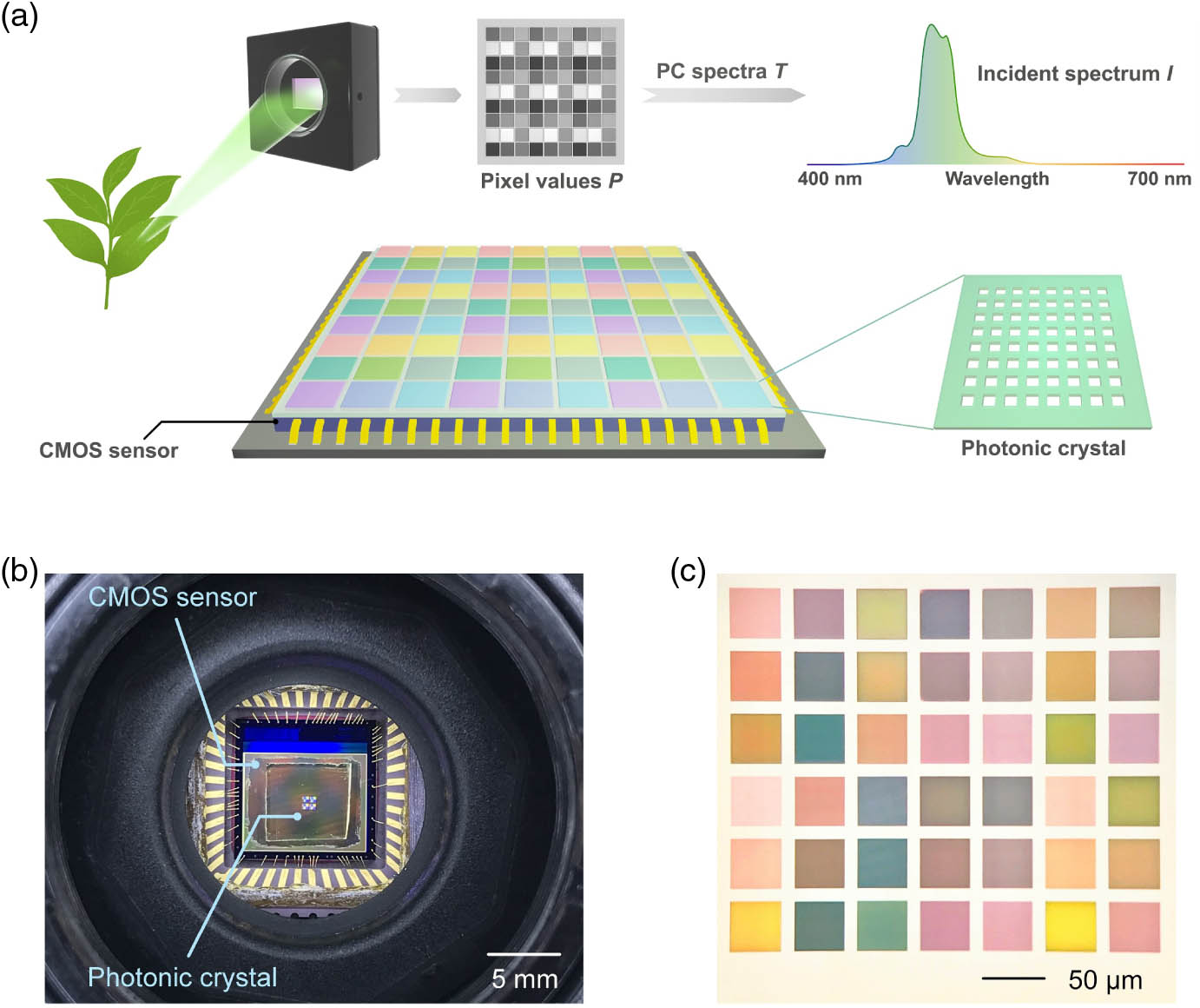
In this paper, we present a compact PC-slab-based CMOS spectral sensor [Fig. 1(a)] for the visible spectrum range (400–700 nm wavelength) with a best spectral resolution of 1 nm. Featuring a small footprint of μμ, the spectral sensor consists of an array of 2D PC slabs atop CMOS photodetectors without mechanically moving parts [Figs. 1(b) and 1(c)]. Unlike most of the traditional spectral sensors that require scanning, our sensor can measure a spectrum in a single shot.
Figure 1.Sensor operating principle and device images. (a) Sensor operating principle and schematics. The spectral sensor consists of an array of PC slabs atop a CMOS image sensor. The transmission spectra of the PC slabs differ significantly from each other and form a sampling basis . For an incident light, the pixel values of the sensor and the sampling basis are used to infer the unknown spectrum of the light. (b) Device photograph. The sensor consists of an array of PC slabs fabricated on a substrate, placed on a CMOS image sensor. (c) Optical micrograph of a PC slab array.
Each PC slab is designed to exhibit a unique transmission spectrum. The spectra of all the PC slabs exhibit a diverse range of spectral features and constitute a sampling basis (). To measure an unknown light spectrum (), the CMOS light-sensing pixels measure the intensity of the light transmitted through the PC slabs. Unlike the sampling basis used in conventional spectrometers, such as narrow bandpass filters, our sampling basis relies on randomness to create uncorrelated features over a wide range, rendering it appropriate to use advanced signal processing methods such as compressed sensing [18–23] to recover the incident spectrum. The light intensity is an integral of the incoming light intensity multiplied by the transmission of the PC . This integral can be approximated discretely as the sum of the products of light intensity and PC transmission [Eq. (1)], with from to , where is the number of the spectral bands to be reconstructed: The measured signal is a function of the sensitivity of the photodetectors. For simplicity, hereinafter, the transmission of the PC slabs implies the aggregated transmission including the factor of . For a total of different subpixels, an -element vector can be read from the image pixels in a single shot. We can express all the measurements using a set of linear equations . The PC transmission matrix is obtained from calibration. Our goal is to solve for the unknown spectrum . It is generally an underdetermined problem that can be solved using many existing techniques [18].
Sign up for Photonics Research TOC. Get the latest issue of Photonics Research delivered right to you!Sign up now
B. Numerical Simulation
To maximize the likelihood of a successful reconstruction of , each row in the matrix should exhibit minimal correlation. This can be realized by designing the transmission spectra of the PC structures to exhibit as many random and uncorrelated features as possible. Hence, we used a high-index material as the PC slabs because it supports more resonant modes, and therefore more spectral features. It is noteworthy that the spectral randomness and total transmitted signal intensity are degraded by light absorption by materials of the PC slabs. Among typical Si-based dielectrics and semiconductors, exhibits both a reasonably large real part and a small imaginary part of the refractive index. It can be used to create highly random transmission spectra into the short wavelength range and encompass the entire visible spectrum of 400–700-nm wavelength. Furthermore, as is typically used as anti-reflection coating on CMOS imaging sensors, it is readily available in the CMOS fabrication process.
To obtain more insights on whether is more appropriate than other Si-based materials for the spectral sensor, we first theoretically studied the performance of four materials including amorphous Si (-Si), silicon carbide (SiC), silicon dioxide (), and . In our simulation, the device from the top to the bottom consisted of a 400 nm thick layer, a 1 μm thick layer, and a silicon substrate. The transmission spectra were measured at the interface of the glass and the silicon substrate. Figure 2(a) shows the experimentally measured real parts () and imaginary parts () of the refractive indices of these four materials deposited using chemical vapor deposition. As evident from its large value (), -Si would be strongly absorptive at wavelengths shorter than 550 nm, rendering it ineffective for spectral reconstruction in that range. More quantitatively, we studied the performances of SiC, , and in spectral sensing. We chose 42 different PC structures by linearly varying the period of the rectangular lattice from 0.4 to 1.0 μm. Additionally, square holes or pillars of lengths ranging from 80 to 700 nm were patterned at the centers of the PC unit cells. For these three materials, the same set of 42 PC geometries was used to build the sampling basis in the 400–700-nm wavelength range with a step of 1 nm. The overall spectral profile was affected mainly by the lattice periodicity, while it was less sensitive to the center pattern geometry. Thus, slight variation in the center pattern geometry would not drastically impact the sensing performance and we did not perform finer tuning of the geometry other than varying the period size. Figure 2(b) presents the simulated transmission spectra of the PC slabs. As expected, the and PC slabs indicated higher transmissions than the SiC PC slabs, particularly at shorter wavelengths, while the SiC spectra were more random at longer wavelengths.
Figure 2.Transmission of PC slabs fabricated using different materials. (a) The real parts and imaginary parts of refractive indices for α-Si, , SiC, and deposited using chemical vapor deposition. (b) Representative transmission spectra for , , and SiC by numerical simulation. (c) Mapping of correlation coefficients between each pair of the 42 simulated transmission spectra in different wavelength ranges. Blue indicates weak or negative correlation; red indicates strong positive correlation. For each mapping plot, the value on the secondary diagonal is the mean value of this matrix.
To further characterize the performance of these materials, we performed spectral sensing in 400–500 nm, 500–600 nm, and 600–700 nm wavelength ranges, corresponding to the blue, green, and red tinges, respectively. Figure 2(c) presents the mapping of the correlation coefficients for each pair of two rows in the matrix in different wavelength ranges, where is the transmission of the th PC slab, indicates the average, and indicates the standard deviation. Statistically, an value smaller than 0.5 indicates a moderate or weak correlation; therefore, in Fig. 2(c), the blue corresponds to values smaller than 0.5 and indicates good designs. For the entire 400–700-nm spectral range, the mean values of the correlation coefficient are 0.84, 0.49, and 0.35 for PC slabs fabricated using SiC, , and , respectively. Specifically, for the SiC PC slabs, the undesirable high correlation is due to the strong absorption in the shorter wavelength range. For the PC slabs, the correlation increases significantly in the longer wavelength range because, for a given film thickness, a small refractive index can support fewer number of optical modes in the long wavelength range than in the short one. Overall, the matrix of the PC slabs maintains low mutual correlation values in all spectral ranges and is most promising for spectral recovery.
Next, we reconstructed the simulated optical spectra using these matrices. Figure 3(a) plots the reconstruction results of simple spectra in the 400–500 nm, 500–600 nm, and 600–700 nm wavelength ranges. The matrices () included the spectra of all of the 42 PC structures in the wavelength range of 400–700 nm with a step of 1 nm. Furthermore, we included measurement noise in our simulation. We added random noises of relative amplitude within to both the calibration and measurement processes. The underdetermined equations were solved subject to regularizations as detailed in Refs. [18,19], exploiting the mathematical properties of the spectra (e.g., the smoothness) as prior knowledge. For both the and PC slabs, their matrices reconstructed the spectra in all of the three wavelength ranges excellently, with errors . The SiC PC slabs could recover the spectra with high accuracy in the 600–700 nm range but the error increased significantly for the shorter wavelengths, which was respectively 4.2% and 35% for the 500–600 nm and 400–500 nm ranges. It is expected that the SiC PC slabs would produce less accurate results than the and , because in general the smaller correlation should benefit reconstruction. It is counterintuitive that although the correlation of the SiC matrix in the 400–500-nm range was significantly smaller than in the 500–600-nm range, the reconstruction error in the 400–500-nm range was much larger. Such a large error should be attributed to the high absorption of SiC in the short wavelength range, where the signal is much more susceptible to noise, resulting in a severely degraded reconstruction. Therefore, an ideal material to develop the PC slabs should exhibit both a large real part and a small imaginary part of the refractive index. At short wavelengths, the optical absorption becomes the limiting factor. In addition to using 42 PC slabs for reconstruction, we also studied the effect of reducing the number of PCs. It is highly desirable to use as few PC slabs as possible, which would maximize the spatial resolution that the sensor could offer for hyperspectral imaging. Figures 3(b) and 3(c) indicate that when the number of PCs was reduced from 42 to 12, the -based structure maintained a much higher reconstruction accuracy than and SiC, thus is more appropriate for developing hyperspectral sensing and imaging devices.
Figure 3.Simulated spectra reconstruction results. (a) Reconstruction of a three-peak spectrum in different spectral ranges using three different materials. SiC-based PC exhibits large error in the 400–500-nm range. (b) and (c) Reconstruction of a more complex spectrum using fewer PC slabs. The PC slab achieves significantly higher reconstruction accuracy than and SiC when the PC number is reduced to 12. The reconstruction error presented here is calculated using , where is the simulated spectrum, is the reconstructed spectrum, and indicates the L-1 norm of . In (a) and (b), the solid lines indicate original simulated spectra, while circles represent recovered spectra.
Experimentally, we fabricated PC slabs using and reconstructed both narrowband and broadband spectra in different wavelength ranges. A 400-nm-thick was first deposited on a fused quartz substrate. The pattern on the was defined lithographically and transferred onto the layer using reactive ion etching. The fabricated PC slabs were then attached to the CMOS sensor for measurements. Figure 4(a) shows an image captured at the wavelength of 450 nm using the PC slab-mounted sensor. Four PC arrays were fabricated on this chip, with each array containing 42 PC structures. Within each array, small squares with different gray-scale values indicate the different transmission rates of the PC structures at this wavelength. Figure 4(b) is a scanning electron microscopy image showing the detailed geometry of a representative PC structure, while Fig. 4(c) is the transmission spectrum of this PC structure measured using our CMOS image sensor. The transmission spectra of the PC slabs were calibrated using a monochromator, which output monochromatic light of wavelength from 400 to 700 nm at a step of 1 nm. The exposure time of the CMOS image sensor (8 bits) was a constant and set to ensure that the highest pixel reading in all of the images did not exceed 255, so that the pixel readings reflected the intensity of the light received at different wavelengths. As the intensity of the monochromatic light output from the monochromator differed at each wavelength, the pixel values directly read from CMOS sensor images were corrected by dividing the light intensities measured using a calibrated powermeter such that the previous equations would still be valid.
Figure 4.Experimental results. (a) Image captured by the PC-slab-mounted CMOS image sensor at an illuminating wavelength of 450 nm. (b) Scanning electron microscopy image of a PC slab. (c) Normalized transmission spectrum of the PC in (b) as measured using the CMOS image sensor. The as-measured data are divided by the measured light power at each wavelength to achieve the corrected data for spectral reconstruction. (d) Sensing of monochromatic light using the single-shot sensor. (e)–(h) Spectral sensing using 42 and 9 PC slabs. (e) and (f) Sensing of narrowband (bandwidth ) spectra at 450 and 600 nm, respectively. (g) and (h) Sensing of broader band (bandwidth ) spectra at 500 nm. The spectrum of (g) is achieved using a bandpass filter, while the spectrum of (h) is from a stack of colorful plastic films.
The spectral resolution of the sensor was characterized using monochromatic light [Fig. 4(d)]. The recovered spectra correctly identified the center wavelengths, and small shifts of 1 nm in the center wavelength were unambiguously resolved from the reconstructed spectra. This benchmarks the resolution against the previous device employing Si PC slabs [19]. Figures 4(e) and 4(f) present the narrow spectral peaks measured by the powermeter and recovered using our miniaturized spectral sensor. The spectra were produced using bandpass filters with a full width at half-maximum (FWHM) of 10 nm, centered at 450 and 600 nm, separately. As suggested by the simulation, significantly less than 42 PC slabs can be used for spectral sensing. Indeed, we demonstrated that the spectra recovered using as few as nine PC structures excellently matched the ground truth. This was further corroborated by measuring a bandpass spectrum centered at 500 nm with a broader FWHM of 40 nm [Fig. 4(g)].
Finally, we tested our spectral sensor on a sample fabricated using a stack of colorful plastic films. As shown in Fig. 4(h), the spectrum of the plastic film stack primarily comprises a peak centered at 500 nm with an FWHM of 40 nm; however, the profile was different from that of the 500 nm bandpass filter. In addition, unlike the bandpass filters above that suppressed the transmission to below 0.01% outside the transmission band, the plastic films could not block the optical waves well. Weak but legible signals spanning the entire 400–700-nm range existed, except for the major peak centered at 500 nm. In fact, most materials and objects around us can reflect or transmit light waves in spectral ranges other than those corresponding to our eye colors. Both spectra recovered using 42 and 9 subpixels reproduced the features of the spectra measured using a powermeter, including the weak signals outside of the range of the 500 nm peak. This also implies that in practical applications, prior knowledge about the spectrum to be measured may be required to solve the underdetermined problem.
3. SUMMARY
To summarize, our compact CMOS-based spectral sensor could recover the spectra over the visible light range (wavelength 400–700 nm) for both narrowband and broadband signals. Furthermore, we demonstrated the use of a PC slab array to recover 301 spectral bands by exploiting the mathematical properties of the incident spectral signal, such as the smoothness. Although each of the PC slabs presented in this work is still larger than a single pixel, the PC structure geometries can be further refined to shrink the area of the nanostructures without drastically changing the overall profile of the PC spectra. Also, the period sizes (400–1000 nm) used in this work may be further reduced as allowed by more advanced, industrial fabrication tools. Thus, it is possible to eventually scale the footprint of a PC slab to a single pixel level (2–5 μm). As such, the PC-slab-based CMOS image sensors would enable hyperspectral imaging without exaggeratedly sacrificing the spatial resolution. On the other hand, PC nanostructures can be fabricated monolithically on photodetectors, making inexpensive manufacture possible. Therefore, our device provides a low cost, compact, and portable solution to spectral sensing needs in a wide range of applications, such as in remote sensing, pattern recognition, and industry inspection.