High-quality holmium-doped (YAG) ceramic is fabricated in sequence by tape-casting and vacuum sintering. The average grain size of the Ho:YAG ceramic is around 20 μm with a fully dense microstructure. The inline transmittance of the sample is in visible and IR region. The fluorescence lifetime at 2088 nm is 8.17 ms. The excellent properties of the Ho:YAG ceramic demonstrate the tape-casting is a novel candidate process for the fabrication of Ho:YAG-based thin-chip or composite ceramics.
(YAG) transparent laser ceramics have been widely studied[1–4] since Ikesue et al. first achieved 1064 nm lasing on Nd:YAG ceramics in 1995[5]. YAG-based ceramics have proven to be one of the most promising materials for applications for solid-state lasers. Lasers peaking at various wavelengths could be obtained by introducing into YAG different kinds of rare-earth ions[6–8]. Compared with those at other wavelengths, laser emission at is more attractive for various applications, including laser radar, coherent lidar, and pumping source for mid-IR optical parametric oscillators (OPOs), because of its eye-safe nature, and high absorption rate in water and human tissues[9–13]. It is well-known that holmium-ion-doped YAG is suitable for producing laser emission due to the manifold transition[14–16]. Yang et al. reported a maximum output power of 2.97 W for 1.0 at.% Ho:YAG with laser wavelength peaking at about 2098 nm[17].
Several forming methods for YAG-based ceramics have been introduced, such as dry-pressing[18,19], slip-casting[20–22], and tape-casting[23–25]. The first two methods are superior in fabricating ceramics of large size and regular shapes. However, there are some problems with preparing thin-chip ceramics or materials with composite structure. Composite green-bodies prepared by these two methods are at least several millimeters thick. Also, irregular interfaces between the adjacent layers in the ceramics with composite structure will significantly lower the optical performance[26]. Tape-casting is nonetheless a good choice for fabricating ceramics with a thin-chip or composite multilayer structure. The first application of tape-casting on YAG-based ceramics (Nd:YAG) was reported by Lee et al. in 2009[27]. Ter-Gabrielyan et al. reported the first laser operation of tape-casting composite ceramic Er:YAG rod[28]. Tang et al. prepared YAG/Yb:YAG/YAG with gradient structure by tape-casting and observed laser output[29]. To date, to our knowledge, there has not been any report on applying tape-casting to preparation of Ho:YAG ceramics. In this work, highly transparent 1 at.% Ho:YAG ceramic with laminated structure was successfully fabricated by tape-casting and vacuum sintering. The microstructure and optical properties were investigated systematically.
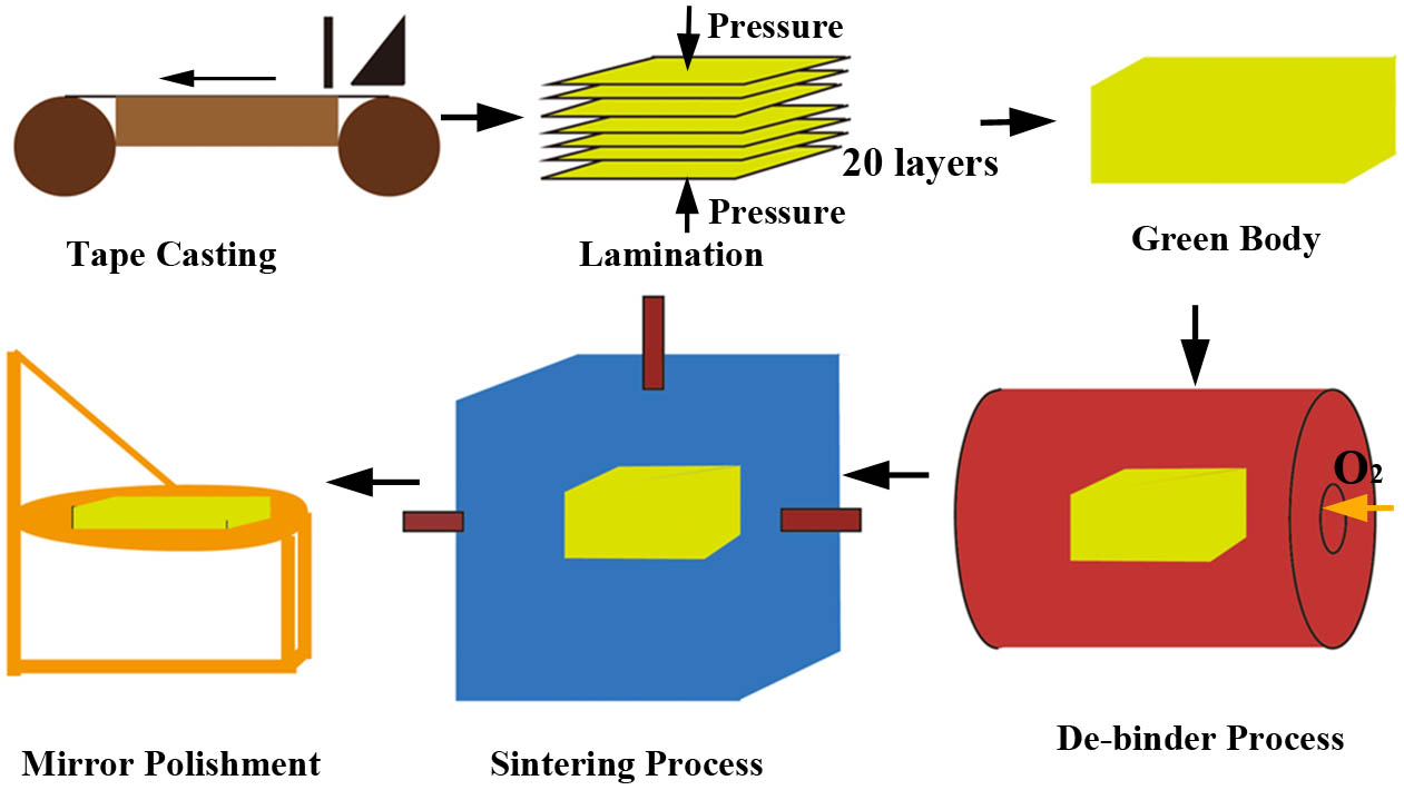
As shown in Fig. 1, the process of synthesizing 1 at.% Ho:YAG transparent ceramic was similar to the method reported in Ref. [30]. High-purity powders of , , and were used as raw materials. These powders were weighed according to the chemical stoichiometric , followed by a two-step ball-milling in agate jar. Mixture of ethanol and xylene in equal mass was used as solvent. Before the first step, fish oil and tetraethyl orthosilicate (TEOS) were added into the slurry, acting as dispersant and sintering aid. Polyvinyl butyral (PVB) and cyclohexanone were added into the slurry and used as binder and plastic agent before the second round ball-milling process. After eliminating the air in the slurry, the tape-casting process was carried out with a blade gap of 600 μm. The thin tapes were further cut into small pieces. Twenty layers of these pieces were stacked together and pressed into a sheet. The organic content was burned off at 800°C in oxygen atmosphere before cold-isostatic press. The green body was vacuum sintered at 1780°C for 20 h prior to the annealing treatment at 1450°C for 10 h. Both surfaces were mirror-polished for optical measurement.
Sign up for Chinese Optics Letters TOC. Get the latest issue of Chinese Optics Letters delivered right to you!Sign up now
Figure 1.Schematic diagram of the ceramic fabrication process.
The crystal structure of the sample was detected by X-ray diffraction (XRD; MiniFlex II, Rigaku). The microstructure of surface was tested by scanning electron microscopy (SEM; JSM-6700F, JEOL). The optical transmittance was measured by UV/visible/near infrared reflection (NIR) spectrophotometer (Lambda-900, PerkinElmer). The fluorescence spectra and decay curves were recorded by a spectrophotometer (Edinburgh, FLS920) with an OPO laser as the exciting source. The signals were detected by a NIR photomultiplier tube (PMT; Hamamatsu, R5509).
Figure 2 shows the XRD pattern of the Ho:YAG ceramic. Compared with pure YAG (powder diffraction file (PDF) card, 88-2048), no diffraction peaks of other phases is observed in the XRD result.
Figure 3 shows the SEM image of the polished surface morphology of the Ho:YAG ceramic by tape-casting. The fully dense microstructure with an average grain size of about 20 μm is observed in the Fig. 3. The whole structure is clean, as neither pores nor second phases are spotted. Such excellent microstructure ensures the high optical transmittance that is shown in Fig. 4.
Figure 3.SEM image of the Ho:YAG ceramic after thermal etching for 10 h at 1450°C.
Figure 4(a) shows the inline transmittance spectra of the tape-casting Ho:YAG ceramic between 200 and 2200 nm. Figure 4(a), inset, shows the photo of the Ho:YAG ceramic with a thickness of 2 mm. It can be found that the ceramic is of high transparency, as the transmittance is as high as 82%, both in the visible and IR spectral region, which reaches the upper limit of the theoretical value[31]. Figures 4(b) and 4(c) show the transmittance spectra ranging from 350 to 600 nm and 1800 to 2000 nm, respectively. The absorption peaks at 450 and 1908 nm correspond to the electronic transition of ion manifolds , and , respectively. As shown in Fig. 4(a), the small absorption observed at 2088 nm will be discussed in a subsequent paragraph.
In order to obtain more reliable information about the perspective of our material, we calculated the absorption cross section and emission cross section. Figure 5 shows the absorption and emission cross section of the tape-casting Ho:YAG ceramic. The absorption cross section was calculated by[32]where is the ionic concentration in the material (), and represents the absorption coefficient of the Ho:YAG ceramic, which could be identified by where is the transmittance of the ceramic, and is the thickness of the ceramic. The emission cross section was calculated by[33]where and are the partition functions for the lower and upper levels, respectively (, and ); ()[32] is the energy for the transition between the lower Stark sublevels of the emitting multiplets and the lower Stark sublevels of the receiving multiplets (zero-phonon line); h is the Planck constant; c is the light speed in air; k is the Boltzmann constant; is the temperature (room temperature in this work).
Figure 5.Absorption and emission cross section spectra of in the YAG ceramic.
The absorption cross section at 1908 nm and emission cross section at 2088 nm are and , respectively. The result is agree with the work reported by Kwiatkowski et al.[34]
Figure 6 shows the measured fluorescence emission spectra of the tape-casting Ho:YAG ceramic in the range of 1800–2200 nm, excited by an OPO laser at 450 nm. The emission peak at 2088 nm, with FWHM of 30 nm arising from the manifold transition of .
Figure 6.Emission spectra of the Ho:YAG ceramic excited at 450 nm.
Figure 7 depicts the fluorescence lifetime of the tape-casting Ho:YAG ceramic. By fitting the decay curve with a single exponential function [], we determine the fluorescence lifetime of the Ho:YAG ceramic, which is 8.17 ms, a little smaller than 8.37 ms, which was obtained by Kwiatkowski et al.[35]. Based on the transmittance spectra shown in Fig. 4(a), the transmittance at 2088 nm is 79.13%. The self-absorption effect occurs at 2088 nm for the Ho:YAG ceramic, leading to a longer lifetime than that of Nd:YAG, Yb:YAG ceramics[36,37].
Figure 7.Fluorescence lifetime of the Ho:YAG ceramic at 2088 nm.
In conclusion, highly transparent polycrystalline 1 at.% Ho:YAG ceramic is successfully fabricated by tape-casting and vacuum sintering. The microstructure and optical properties are investigated. Pore-free and fully dense Ho:YAG ceramic with an average grain size of about 20 μm is obtained after sintering at 1780°C for 20 h. Close to the theoretical value, the inline transmittance with thickness of 2 mm is about 82% both in visible and IR region. The fluorescence at 2088 nm indicates a superior NIR emission with maximum emission cross section of . Due to the self-absorption effect, the upper state lifetime at 2088 nm is 8.17 ms. The excellent optical performance of the Ho:YAG ceramic in this work demonstrates that the tape-casting is a promising alternative technology for preparing thin-chip Ho:YAG ceramics or Ho:YAG-based ceramics with composite structure.