Author Affiliations
1Laboratory of Micro-Nano Optoelectronic Materials and Devices, Shanghai Institute of Optics and Fine Mechanics, Chinese Academy of Sciences, Shanghai 201800, China2Center of Materials Science and Optoelectronics Engineering, University of Chinese Academy of Sciences, Beijing 100049, China3National Center for Protein Science Shanghai, Shanghai 200120, China4Wuhan National Laboratory for Optoelectronics, Huazhong University of Science and Technology, Wuhan 430074, China5Shenzhen Huazhong University of Science and Technology Research Institute, Shenzhen 518057, Chinashow less
Abstract
In this Letter, a new approach of optical tape for high capacity multilayer data storage is proposed. We show that a length of 5 cm and width of 2 cm of soft and transparent optical tape can be used for two-photon three-dimensional bit data storage. We successfully demonstrate writing and reading of six layers of data storage with a transverse bit separation of 2 μm and an axial separation of 2.5 μm in a tetraphenylethylene-doped photobleaching polymer. The fluorescence intensity is insensitive to the storage depth of the photopolymer matrix. Thus, the optical tape that we put forward in the experiment can help people realize true large data storage in the future, like magnetic tape. This method significantly paves a novel way for solving big data storage problems.Three-dimensional (3D) optical data storage (ODS) has been studied by many researchers in order to overcome the data storage problem and lead to transformative advances in the data storage field[1–8]. Compared with holographic memory[9,10], ODS has been shown to be superior because of its high tolerance to vibration and robust reliability. The capacity is limited, however, by the size of the storage matrix and the number of layers in these media. Although magnetic tape is the mainstream storage method and has high storage capacity, the ultralow lifespan and significant high energy consumption impede the more widespread application in the future. Here, we report on a photocuring process for fabricating optical tape film for high density ODS. Optical tape has the potential of high storage capacity like magnetic tape, as well as ultralong lifetime and low energy consumption. The photocuring process is with low cost and far simpler than current manufacturing approaches, such as spin-coating[4,11], lamination[11–13], and co-extrusion[14,15], which are intricate and not easily scalable.
Photocuring, also ultraviolet (UV)-curing, technology is a kind of curing technology that transforms the liquid epoxy acrylic resin into a solid state at a high speed (usually several seconds) by UV irradiation of a certain wavelength. The essence of UV-curing is photopolymerization and crosslinking reactions. In the photocuring system, 1173 2-hydroxy-2-methylpropiophenone (HMPP) is one of the most successful photoinitiators. Thus, HMPP will act as the photoinitiator in our optical tape data storage experiment.
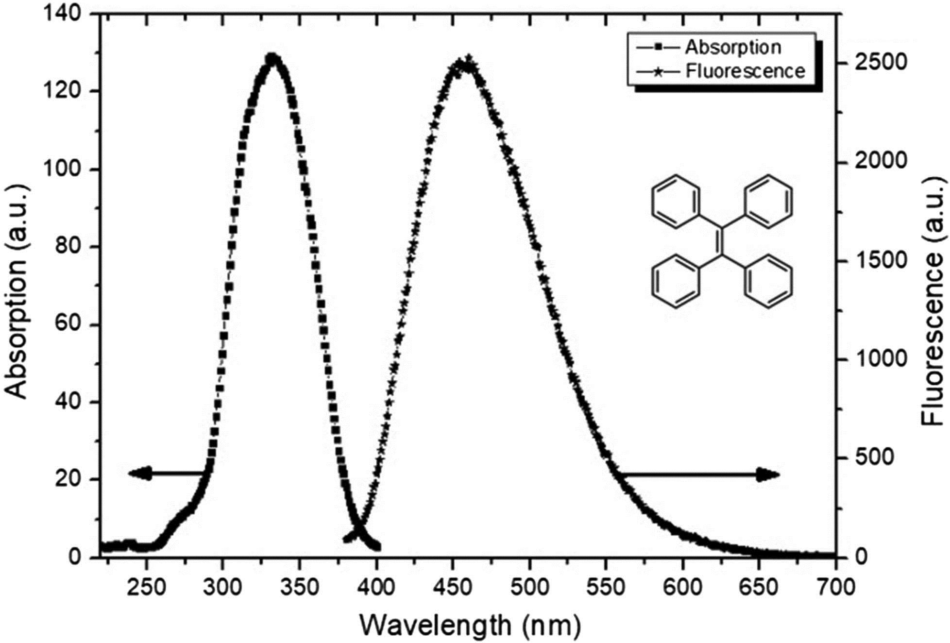
In recent years, bit-by-bit ODS based on photopolymerization has been the most popular method. The key to the success of this method is the monomer host material[16–18]. What we use in the experiment is this five-functional monomer dipentaerythritol pentaacrylate (DTPA); many research groups[5,18,19] have utilized it to realize binary ODS through many ways. Although DTPA is suitable for data storage, the detection way of stored data greatly limits the widespread applications. Fluorescence detection as an information readout method is capable of attaining a higher contrast or signal-to-noise ratio than the traditional scanning electron microscope (SEM) readout method. Thus, fluorescent dye tetraphenylethylene (TPE), which is a white powder, is added into our photopolymerization system to fabricate a transparent photopolymer film. Figure 1 shows the absorption and fluorescence emission spectrum curves of TPE powder with the maximum emission wavelength at 450 nm when the excitation wavelength is 365 nm. The inset in Fig. 1 shows the TPE molecule structure that we used in the experiment.
Sign up for Chinese Optics Letters TOC. Get the latest issue of Chinese Optics Letters delivered right to you!Sign up now

Figure 1.TPE absorption and fluorescence spectra. The inset shows the TPE molecule structure.
Designing optical tape material is the first step in this process. To prepare the photoresist compound, the monomer DTPA, photoinitiator HMPP, and fluorescent dye TPE, which are transparent and thermostable, were dissolved in acetone. They were kept in the oven at the temperature of 50°C for 12 h to remove acetone[17] and fabricate highly thick photoresist. At last, the photoresist compound contained monomer 98 wt.%, HMPP 1.5 wt.%, and TPE 0.5 wt.%, respectively. We fabricated an optical tape storage medium by dropping about 2 mL photoresist matrix on a glass slide, and another glass slide was pressed to sandwich the photoresist between two glass slides separated by a 40 μm thick sticky-tape spacer. Thus, the optical tape is about 6 cm long, 2 cm wide, and 40 μm thick. The schematic and the photograph of sample film produced in this study are shown in Figs. 2(a) and 2(b), respectively. The optical tape in Fig. 2(b) shows a cyan color because it was illuminated under UV light. Usually, the photocuring system materials are much tougher; however, they will become soft and elastic if they are thin enough.
Figure 2.(a) Schematic of setup used to manufacture the films and (b) the result of optical tape film.
We utilized high-power UV light to radiate the liquid photopolymer for different times to fabricate solid films of different curing degrees. The exposure times were 5 s, 10 s, 15 s, and 20 s, respectively. We then tested the average fluorescence intensities of the four solid films, and the normalized fluorescence intensities are shown in Fig. 3. The fluorescence intensity gradually increases with the increase of the curing degree because of the aggregation-induced emission attribute[20,21] and reaches the maximal value when the radiation time is 15 s. However, the fluorescence intensity will decrease if we continuously increase the exposure time to 20 s. This may be because of the photobleaching of the TPE dye caused by high power UV radiation, and further researches need to be conducted. Thus, we chose 15 s as the best exposure time when we performed the data storage experiment.
Figure 3.Normalized fluorescence intensities of solid films of different curing times.
The data writing was performed by using two-photon photobleaching when the laser wavelength is 515 nm. The laser light was focused into the polymer block through a high numerical aperture (NA) oil lens. The photopolymer compound material that we used was a polymer doped with a dye that can be excited by two-photon absorption[22] because TPE has certain absorption at the position of 257.5 nm, which we can see from Fig. 1. The places that have been bleached show up as darker areas than the surrounding fluorescent area. As a consequence, the information is recorded as bleached patterns under two-photon excitation.
The results for writing and reading two-photon 3D data storage at different depths in the polymer under femtosecond (fs) illumination are shown in Fig. 4. The average exposure power was 20 mW, and the exposure time was 30 ms, respectively. Six layers of data bits were recorded with a transverse bit separation of 2 μm and layer separation of 2.5 μm, and the different colors represent the different storage depths. In this case, the recorded information can be read out in confocal fluorescence microscopy. We also recorded data points at corresponding layers. From Fig. 5, we can see that the fluorescent signals do not have a significant reduction in the layer at a deeper position in the polymer. The fact of no noticeable cross talk between layers in Fig. 5 suggests that the layer separation could be reduced further.
Figure 4.Recording and readout result of six recording layers under two-photon illumination in the photobleaching polymer. The spacing between adjacent layers is 2.5 μm. (a) The first layer, also the lowest layer, including the digit number 1; (b) the second layer, including the digit number 2; (c) the third layer, including the digit number 3; (d) the fourth layer, including the digit number 4; (e) the fifth layer, including the digit number 5; (f) the sixth layer, also the topmost layer, including the digit number 6.
Figure 5.Fluorescent signals of different storage depths.
In conclusion, we have demonstrated fabrication and use of a novel 3D optical storage medium. Optical tape can be easily made in just several seconds. We have written in films containing six layers with digit numbers and data points and read using confocal fluorescent microscopy. We can store nearly 16 layers in a 40 μm thick photopolymer matrix, and the storage capacity can reach approximately . Finally, it should be pointed out that the optical tape in this experiment is just several centimeters. Although we can achieve 3D ODS, the storage capacity is far from meeting storage requirements. Thus, improving the length of optical tape is the subject of our ongoing research and aims to realize petabyte (PB) storage capacity. We are doing researches about super-resolution optical storage experiments now, and we firmly believe that the storage capacity can reach exabyte (EB) in the future.
References
[1] A. S. Dvornikov, E. P. Walker, P. M. Rentzepis. J. Phys. Chem. A, 113, 13633(2009).
[2] W. Dallari, M. Scotto, M. Allione, E. Samoylova, F. Pignatelli, R. Cingolani, A. Athanassiou, A. Diaspro. Microelectron. Eng., 88, 3466(2011).
[3] S. Kawata, Y. Kawata. Chem. Rev., 100, 1777(2000).
[4] M. Nakano, T. Kooriya, T. Kuragaito, C. Egami, Y. Kawata, M. Tsuchimori, O. Watanabe. Appl. Phys. Lett., 85, 176(2004).
[5] M. M. Wang, S. C. Esener. Appl. Opt., 39, 1826(2000).
[6] K. Zhang, J. C. Lin, Y. Wang. Chin. Opt. Lett., 13, 121601(2015).
[7] D. A. Parthenopoulos, P. M. Rentzepis. Science, 245, 843(1989).
[8] K. Wang, W. Zhang, Z. Y. Zhou, M. X. Dong, S. Shi, S. L. Liu, D. S. Ding, B. S. Shi. Chin. Opt. Lett., 15, 060201(2017).
[9] R. R. McLeod, A. J. Daiber, M. E. McDonald, T. L. Robertson, T. Slagle, S. L. Sochava, L. Hesselink. Appl. Opt., 44, 3197(2005).
[10] X. Lin, Y. Huang, Y. Li, J. Y. Liu, J. P. Liu, R. D. Kang, X. Q. Tan. Chin. Opt. Lett., 16, 030501(2018).
[11] P. Zijlstra, J. W. M. Chon, M. Gu. Nature, 459, 410(2009).
[12] M. Miyamoto, M. Nakano, M. Nakabayashi, S. Miyata, Y. Kawata. Appl. Opt., 45, 8424(2006).
[13] A. Ohta, M. Miyamoto, Y. Kawata, M. Nakabayashi. IEEE Trans. Magn., 43, 832(2007).
[14] C. Ryan, C. W. Christenson, B. Valle, A. Saini, J. Lott, J. Johnson, D. Schiraldi, C. Weder, E. Baer, K. D. Singer, J. Shan. Adv. Mater., 24, 5222(2012).
[15] C. W. Christenson, A. Saini, B. Valle, J. Shan, K. D. Singer. J. Opt. Soc. Am. B, 31, 637(2014).
[16] T. F. Scott, B. A. Kowalski, A. C. Sullivan, C. N. Bowman, R. R. McLeod. Science, 324, 913(2009).
[17] Y. Y. Cao, Z. S. Gan, B. H. Jia, R. A. Evans, M. Gu. Opt. Express, 19, 19486(2011).
[18] Z. S. Gan, Y. Y. Cao, R. A. Evans, M. Gu. Nat. Commun., 4, 2061(2013).
[19] X. P. Li, Y. Y. Cao, N. Tian, L. Fu, M. Gu. Optica, 2, 567(2015).
[20] Y. Q. Dong, J. W. Y. Lam, A. J. Qin, J. Z. Liu, Z. Li, B. Z. Tang. Appl. Phys. Lett., 91, 011111(2007).
[21] Y. B. Hu, J. W. Y. Lam, B. Z. Tang. Chin. J. Polym. Sci., 37, 289(2019).
[22] M. Gu, D. Day. Opt. Lett., 24, 288(1999).