1School of Electrical and Computer Engineering and Inter-University Semiconductor Research Center, Seoul National University, Gwanak-Gu Gwanakro 1, Seoul 08826, South Korea
2School of Electronics Engineering, Kyungpook National University, Daegu 41566, South Korea
Chulsoo Choi, Sun-Je Kim, Jeong-Geun Yun, Jangwoon Sung, Seoul-Yeol Lee, Byoungho Lee. Deflection angle switching with a metasurface based on phase-change nanorods [Invited][J]. Chinese Optics Letters, 2018, 16(5): 050009
Copy Citation Text
We propose the active metasurface using phase-change material (GST), which has two distinct phases so called amorphous and crystalline phases, for an ultrathin light path switching device. By arranging multiple anisotropic GST nanorods, the gradient metasurface, which has opposite directions of phase gradients at the two distinct phases of GST, is demonstrated theoretically and numerically. As a result, in the case of normal incidence of circularly polarized light at the wavelength of 1650 nm, the cross-polarized light deflects to at the amorphous phase and at the crystalline phase with the signal-to-noise ratio above 10 dB.
Optical elements presenting active characteristics are essential components that increase throughput of optical data processing. Light path switching devices that actively modulate the direction of light propagation, especially, are in high demand for many applications, such as optical communication[1], optical data storage[2], and optical integrated circuit[3]. For a macroscopic optical system, most of these devices are operated by mechanical actuation harnessing geometrical deformation of optical elements[4] or spatial light modulation of flat optic components through an external pump signal[5]. However, it is quite difficult to miniaturize light path switching devices without losing reliable performance, though there is an increasing demand for microscopic optical devices.
Recently, metasurfaces have been intensively investigated and used as substitutions for bulky optical elements in the miniaturization of the optical system. A Metasurface, a flat optical device with sub-wavelength thickness, is composed of periodically arranged nanoantennas to modulate the optical characteristics of an input light signal, such as spectrum, polarization, and wavefront[6–9]. Incorporating optically active ingredients in a metasurface is required for the application of an active optical system. In various active devices, tuning by an external signal has been realized by using non-linear materials[10,11], such as a building block of a metasurface, or by combining functional materials like environmental interacting materials[12–14]. Harnessing the phase-change material, (GST) is the most effective among available approaches, as their high-index contrast characteristics and reversible switching property guarantee reliable switching within nanoseconds[15,16]. Most notably, GST is efficient in terms of power consumption by virtue of its non-volatile phase-change characteristic—it maintains its transited phase even after the external stimuli is ceased[17–19]. Among the studies concerning GST metasurface[20–22], there have been some demonstrations that achieve compact light path switching by Yin et al.[23] and Cao et al.[24]. However, these devices only guarantee small switching angles of 23.6° and 11° for transmitted light with an efficiency about 5%, respectively. Including the work done by Yin et al.[23], previous metasurfaces designed for beam switching are usually demonstrated by simply adding two different types of meta-atoms on a single layer. Therefore, only the half of meta-atoms are dominantly reactive, whereas other half of the meta-atoms are less reactive. These less reactive meta-atoms that transmit light make unavoidable noise that eventually degrade the signal-to-noise ratio and restrict the range of the switching angle.
In this Letter, we propose an active metasurface based on the array of GST nanorods operating at 1650 nm. In the proposed structure, the complex amplitude of transmitted light is determined by both upper and lower meta-atoms, which means that there is no classification of dominantly reactive or less-reactive meta-atoms. Therefore, it can exhibit a very large switching angle of 111.2° without unwanted noise excited by a less-reactive meta-atom with a signal-to-noise ratio above 10 dB, which is numerically verified by using COMSOL multiphysics. By adapting the gradient metasurface concept[25–27], opposite directions of the phase gradient for transmitted cross-polarized light are designed for two distinct phases of GST in case of circularly polarized light incidence.
Sign up for Chinese Optics Letters TOC. Get the latest issue of Chinese Optics Letters delivered right to you!Sign up now
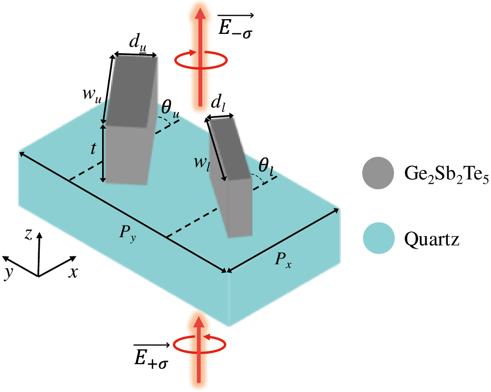
The refractive indices of GST in the crystalline and amorphous phases are , and , respectively, which are referenced from the work by Park et al.[17]. Two different sizes of GST nanorods are located in the unit cell as shown in Fig. 1. When the period of the unit cell (with unit length of and ) is in the sub-wavelength scale, the transmitted cross-polarized light—left-handed circularly polarized (LCP) light follows, as in Eq. (1) when right-handed circularly polarized (RCP) light is normally incident[28]:
Here, refers to the complex amplitude of the transmitted LCP light. Subscripts and indicate the upper nanorod and lower nanorod, respectively, and indicates the phase of GST. The indicates the phase shift of transmitted light, and subscripts and indicate the space-varying fast axis and slow axis of each nanorod, respectively. As shown in Eq. (1), the complex amplitudes of transmitted LCP light from each nanorod are dominantly determined by respective phase shifts for two orthogonal polarizations and . These respective phase shifts are determined by the length of the nanorod to the corresponding polarization direction[28] and the inherent refractive index of the material[29]. In addition, the exponential terms are determined by the angles and , following the principle of the Pancharatnam–Berry phase (geometric phase)[30–32]. Thus, the transmitted LCP light can have two different values and , depending on the size and angle of each of the two GST nanorods. Based on the abovementioned unit cell design method, we design a supercell structure, which has opposite phase gradient profiles of transmitted LCP light for each distinct state of GST. Equally spacing number of unit cells over a super-period () with a relative phase of ± in between adjacent unit cells makes a constant phase gradient when the size of unit cell is in the sub-wavelength scale. Then, the angle of transmitted light according to the angle of incident light is determined by Eq. (2), which is called the generalized Snell’s law[25–27]:
In case of the normal incidence of light to the gradient metasurface that is placed in air, Eq. (1) can be simplified to . Hence, when the phase shift from each unit cell () decreases gradually in the direction of , the angle of transmitted light is determined in the direction and otherwise in the direction.
In the proposed structure, the phase gradient of the supercell is configured by arranging four unit cells that are in the sub-wavelength scale (, ), as shown in Fig. 2(a).
Figure 1.Schematic illustration of the unit cell structure. The denotes the right-handed circularly polarized light, and the denotes the left-handed circularly polarized light.
Figure 2.(a) Schematic illustration of the designed supercell structure that exhibits opposite phase gradient profiles for each phase of GST. Designed four unit cells are arranged in numerical order to the direction. (b) Numerically calculated phase shifts corresponding to each unit cell that are presented by step functions for two respective phases of GST.
The phase shifts of transmitted LCP light corresponding to each unit cell are numerically calculated as in Fig. 2(b), while maintaining uniform amplitude for the respective phases of GST. Following the designed phase gradient profile, the transmitted LCP light deflects to Floquet mode for the amorphous phase and Floquet mode for the crystalline phase.
To specify the geometric parameters of GST nanorods that compose the unit cells, we first calculated the complex amplitude from single GST nanorods according to and values. The thickness of the GST nanorod is determined as 300 nm with the intention of inducing enough cross-polarized light and avoiding resonance in the nanorods for both phases of GST. As shown in Figs. 3(a)–3(d), owing to different optical properties for two distinct phases of GST, the complex amplitude of transmitted LCP light shows different values for each phase.
Figure 3.Variation trend of complex amplitude of transmitted LCP light according to and values for two distinct phases of GST. (a) The phase of complex amplitude and (c) its absolute value at the crystalline phase. (b) and (d) present those of the amorphous phase, respectively. The black rectangles, blue circles (in the middle of each figure), and red circles (in the leftmost of each figure) denote the selected dimensions of GST nanorods.
Based on numerically calculated complex amplitude from single GST nanorods, we locate two GST nanorods into one unit cell. The transmitted LCP light from unit cell 1, consisting of two identical GST nanorods, follows a simplified equation, . Then, the transmitted LCP light from unit cell 1 can be obtained from Figs. 3(a)–3(d) except for the exponential term, which is determined by . In order to satisfy the phase shift difference value of each GST phase shown in Fig. 2(b), the size of the GST nanorods constituting unit cell 1 is equal to , , as denoted with a black rectangle. Next, we designed unit cell 2, which satisfies the phase shift values of Fig. 2(b) and at the same time transmits light having the same amplitude as the amplitude transmitted from unit cell 1. To satisfy this requirement, we design the phasor map of unit cell 2 as shown in Fig. 4(a) by combining two different GST nanorods. The selected dimensions of the upper GST nanorod are same with , , and lower GST nanorod is same with , and , as denoted by blue and red circles in Figs. 3(a)–3(d). The angle of the upper nanorod is determined by to minimize the near-field interaction between adjacent nanorods. Figure 4(b) is a schematic view of unit cell 2 satisfying the phasor map of Fig. 4(a). In unit cell 2, based on these conditions, when changes from 0° to 180°, the phase shift value changes more steeply for the crystalline phase than for the amorphous phase, as shown in Fig. 4(c). At the condition indicated by the vertical dotted line of Fig. 4(c), is 100°, the optical phase difference between two GST phases is nearly , as well as the amplitude values being almost the same. Lastly, we obtain the exact phase shift values of unit cell 1 by determining with 20° to satisfy the phase relation with unit cell 2. Based on the specified geometric parameters of unit cell 1 and unit cell 2, unit cell 3 and unit cell 4 can be easily designed by simply rotating designed nanorods 90°, following Eq. (1). The dimensions of the whole selected nanorods are sufficiently small to minimize the near-field interaction between adjacent nanorods, which result in light distortion.
Figure 4.(a) Desirable phasor map of transmitted LCP light of unit cell 2 for each phase of GST. (b) The schematic illustration of unit cell 2. (c) Phase and amplitude variation plot according to varying for two distinct states of GST. The vertical dotted line indicates the selected angle of .
We execute full-field simulation by arranging the designed supercell structure periodically in case of normal incidence of RCP light. The radiation pattern of transmitted LCP light almost coincides with the result of Eq. (2): for the crystalline phase and for the amorphous phase, as shown in Fig. 5(a). These results are also proven by wavefronts of transmitted LCP light, as shown in Fig. 5(b). The signal-to-noise ratio, which indicates the intensity ratio between the intended Floquet mode and unintended Floquet modes, is calculated as 13 dB for the crystalline phase and 11 dB for the amorphous phase, respectively. It is noteworthy that the designed light path switching device can operate with time scale of nanoseconds by virtue of the ultra-fast switching characteristic of GST through applying electric pulse[33] or optical pulse signals[34,35]. Also, this device is very efficient in terms of power consumption, because the deflection angle is maintained even though the external stimuli has ceased by virtue of non-volatile phase-change characteristic of GST. However, the diffraction efficiency and intensity of the intended Floquet mode need improvement to be used practically as a light path switching device. Owing to structural limitations that cannot excite large cross-polarized light, the diffraction efficiency is 0.5% for the crystalline phase and 0.3% for the amorphous phase. This disadvantage can be eased off by incorporating an intensity amplifier that is widely used for lossy optical data processing systems[36].
Figure 5.(a) Angular radiation intensity pattern of transmitted LCP light for two distinct states of GST and (b) the corresponding LCP electric field profiles.
In conclusion, we propose the compact light path switching device through a GST metasurface that shows a large beam switching angle with a high signal-to-noise ratio. By virtue of its large beam switching angle, the optical system does not need to provide long propagation lengths to avoid cross-talk. Thus, the proposed device is helpful for decreasing the volume of the entire system, as well as the suppression of cross-talk. Also, it can be easily designed by the one-step e-beam lithography process that is widely used for the single layer nanostructure fabrication[37]. The proposed GST metasurface concept has enough potential to be used as an active flat optical element for various applications that demand highly compact light path switching.
Chulsoo Choi, Sun-Je Kim, Jeong-Geun Yun, Jangwoon Sung, Seoul-Yeol Lee, Byoungho Lee. Deflection angle switching with a metasurface based on phase-change nanorods [Invited][J]. Chinese Optics Letters, 2018, 16(5): 050009