Abstract
In this paper, we report an experimental demonstration of enabling technology exploiting resonant properties of plasmonic nanoparticles, for the realization of wavelength-sensitive ultra-minituarized () optical metadevices. To this end, the example of a 1.3/1.6 μm wavelength demultiplexer is considered. Its technological implementation is based on the integration of gold cut-wire-based metalines on the top of a silicon-on-insulator waveguide. The plasmonic metalines modify locally the effective index of the Si waveguide and thus allow for the implementation of wavelength-dependent optical pathways. The 1.3/1.6 μm wavelength separation with extinction ratio between two demultiplexers’ channels reaching up to 20 dB is experimentally demonstrated. The considered approach, which can be readily adapted to different types of material planar lightwave circuit platforms and nanoresonators, is suited for the implementation of a generic family of wavelength-sensitive guided-wave optical metadevices.1. INTRODUCTION
The continuous improvement of fabrication technologies was the main driving factor enabling miniaturization of electronic circuit components to nanometer scale. Similar trends hold also for optical circuits, with many efforts devoted to bridging the gap between photonics and electronics. Because of their massless nature, photons are orders of magnitude less confined than electrons. Even in the case of high-index materials, such as silicon, implementation of optical functions exploiting interference between co- or contra-propagating waves in nanostructured dielectric materials such as photonic crystals [1,2] or similar [3] requires an interaction length of at least several wavelengths.
The change in paradigm brought by the advent of metasurfaces made it possible to control the phase and amplitude of reflected or transmitted waves on a “skin depth” propagation length on the order of /10 [4–8]. Based on this approach, numbers of functionalities targeting flat optics applications have been demonstrated [4–15]. Meanwhile, another possibility for the manipulation of optical flow by means of metasurfaces is to use them in a guided-wave configuration [16–22]. The demonstration of a gradient effective index metalens based on this concept was recently reported [23]. The technological implementation is performed by means of a metasurface made of a 2D array of gold cut wires (CWs) integrated on top of the Si waveguide. The aim of the present work is to provide a further impetus to this direction by introducing the concept of wavelength-dependent optical pathways, distinctly different from the wavelength-dependent angular beam steering effects in photonic crystals [24,25] or bi-directional coupling using plasmonic Fano nanoantennas [19]. To prove the feasibility of the considered approach, we report the design, fabrication, and experimental demonstration of an ultra-compact () demultiplexer (DMUX) operating in the wavelength range 1.3/1.6 μm.
2. METALINES-BASED WAVELENGTH DMUX OPERATION PRINCIPLE, DESIGN, AND MODELING
The operation principle of the reported wavelength DMUX is based on the wavelength-dependent local variation of the hybrid metal–dielectric waveguide effective index () induced by plasmonic nanoresonators. Here, we use metalines made of 1D arrays of gold CWs instead of 2D metasurfaces to modify locally the index of a Si waveguide, creating thus the equivalent of color-sensitive optical fibers into the Si layer. They can serve as building blocks for numbers of guided-wave optical metadevices based on local variation of the effective index.
Sign up for Photonics Research TOC. Get the latest issue of Photonics Research delivered right to you!Sign up now
The schematic of the hybrid metal–dielectric DMUX operating in a guided-wave configuration is shown in Fig. 1(a). Its technological implementation is performed by means of integration of 1D arrays of plasmonic nanoresonators on top of the 220 nm thick silicon-on-insulator (SOI) slab. The dimensions of gold CW plasmonic nanoresonators are adapted to the transmitted wavelengths, around 1.3 μm in one arm and 1.6 μm in the other one. DMUX operation is performed in the fundamental TE polarization mode of the SOI waveguide, i.e., when the direction of the electric field is parallel to the long axis of CWs in order to induce the excitation of localized surface plasmons.
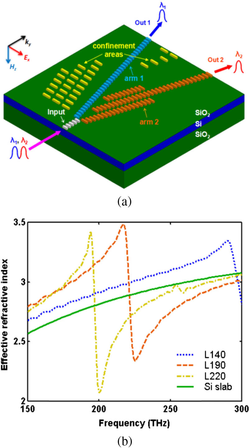
Figure 1.(a) Schematic of integrated hybrid plasmonic–photonic wavelength DMUX. The difference in CWs’ functional roles evidenced by color. (b) Frequency dependence of effective refractive index of the hybrid plasmonic–photonic waveguide for different values of CW lengths: 140 nm, 190 nm, and 220 nm considered here.
The resonant frequency of the localized surface plasmons is the primary parameter for the engineering of such hybrid waveguides’ local effective index. The effective permittivity of the hybrid metal–dielectric slab waveguide can be approximated as the sum of the effective permittivity of the dielectric slab waveguide and Lorentzian-type dispersion formula accounting for the resonant features of plasmonic CWs [22,23]. As shown in Fig. 1(b), the effective refractive index is higher than that of the dielectric slab below the resonant frequency and lower above it. The local value of can thus be on-demand engineered through an appropriate design of resonant element geometry and spatial positioning on the surface of a slab waveguide. Since the resonant frequency of localized surface plasmons is strongly dependent on their dielectric environment, the use of a 5 nm thick interfacial native silicon dioxide layer greatly contributes to increasing CW resonant frequency and facilitates thus the technological fabrication process [22]. However around the resonance frequency of the gold CW occurs a peak of losses. To avoid the detrimental effects of losses inherent to the resonant absorption of metal CWs, it is preferable to detune operation frequency from resonance and find an optimal tradeoff between index variation and loss.
In the present design, the dimensions of CWs used for the 1.3 μm and 1.6 μm output arms are [arm 1 in Fig. 1(a)] and [arm 2 in Fig. 1(a)], respectively. The longitudinal separation distance between the CWs in the direction of wave propagation is 50 nm for the input area metaline and output arms 1 and 2. Concerning the transverse separation distance , it was fixed to 100 nm. For a given CW’s dimensions, the effective index of the hybrid metal–dielectric waveguides, displayed in Fig. 1(b), was determined by means of numerical modeling with a subsequent retrieval procedure [23,26]. Here, for 140 nm and 190 nm CW lengths, the resonance frequencies are 295 THz and 225 THz, respectively.
The role of the additionally implemented -sized CWs, with a resonant frequency around 195 THz, is to enhance the mode confinement of a hybrid plasmonic–photonic waveguide at high frequencies. Indeed, as evident in Fig. 1(b), at the operating frequency of 230 THz, which corresponds to 1.3 μm wavelength, the effective index of the confinement areas () is lower than that of the Si slab (), and than that of arm . In addition, the frequency of 230 THz falls in the highly lossy frequency band of arm 2. This is why the propagation of waves around this frequency in arm 2 is precluded by the resonance of the 190 nm long CWs. This insures that the light is well confined under arm 1. In contrast, at the operating frequency of 188 THz (1.6 μm wavelength), the effective indices of hybrid waveguides with 140 nm and 190 nm long CWs are 2.87 and 3.08, respectively. The light is then redirected into arm 2.
The validity of the effective medium approach results was further verified by full 3D optical simulations of the device. To this end, we performed full 3D high frequency structure simulator (HFSS) [27] simulations with the usual parameters of SOI slab waveguides (2 μm thick buried underclad, 220 nm thick Si core, 5 nm thick overclad corresponding to native oxide). The parameters of Au, Si, and used in HFSS numerical simulations were taken from Palik [28].
The calculated distributions of light intensity at different wavelengths propagating across the hybrid plasmonic–photonic DMUX are shown in Figs. 2(a) and 2(b). A clear spatial separation effect is observed for 1.3 μm (230 THz) and 1.62 μm (185 THz) wavelengths. HFSS numerical simulations show also that the light is correctly guided at each frequency along the corresponding CW metalines.

Figure 2.HFSS modeling results for 1.3/1.6 μm hybrid plasmonic–photonic DMUX. Distribution of propagating light intensity at different wavelengths: (a) (); (b) ().
3. FABRICATION AND EXPERIMENTAL RESULTS
Figure 3 shows the scanning electron microscope (SEM) view of the experimentally fabricated-on-chip DMUX based on the design discussed above: the DMUX is located at the end of a 600 nm wide single-mode waveguide (SMW), and a 500 nm SMW is created at the end of each optical arm to collect the transmitted optical signals. The experimental prototype was fabricated by using a technological process involving two levels of e-beam lithography. The first lithography is dedicated to the definition of the metallic elements pattern, i.e., nano CWs and second mask level alignment marks. This step is performed by means of an NB4 electron-beam lithography setup using PMMA positive resist to define the nanostructure patterns on the surface of an undoped SOI wafer from SOITEC with a 220 nm thick top Si layer and 2 μm Buried OXyde (BOX). It is followed by resist development and double-step e-beam evaporation to deposit a 2 nm film of chromium as an adhesion layer, and then a 50 nm film of gold. The second e-beam lithography is dedicated to Si waveguide pattern definition using a ZEP 520A positive resist. The residual resist is used after development as a soft mask for Si etching. Particular attention should be paid to the high-precision alignment between the nano CWs and Si waveguides patterns. This is achieved by utilizing the metal alignment mark implemented during the metallization step.
Figure 3.SEM image of a fabricated DMUX.
The optical setup employed for the characterization of fabricated wavelength DMUX is illustrated in Fig. 4. Three tunable diode lasers of the T100S series from Yenista Optics used as a light source cover a spectral range from 1.25 μm to 1.68 μm. The linearly polarized light is coupled into a polarization-maintaining lensed fiber that serves for light injection into the waveguide. The light propagating through the DMUX is collected from the silicon chip output side facet by a objective with a 0.6 numerical aperture and then measured with a high-sensitivity 1D CCD array IR camera used for registering the wavelength-dependent spatial distribution of transmitted intensity.
Figure 4.Schematic of the end-fire optical bench setup.
The distribution of light intensity in output waveguides as a function of wavelength is shown in Fig. 5(a). The obtained experimental results bring clear evidence of efficient wavelength separation performed by the DMUX. For wavelengths between 1.25 μm and 1.4 μm, the light propagates in arm 1 with a very weak level of light intensity in arm 2. In contrast, for the wavelengths between 1.6 μm and 1.68 μm, the light propagates mainly in arm 2, while the residual light intensity in arm 1 is very low. To illustrate the efficiency of DMUX wavelength separation, Fig. 5(b) shows superposition of snapshots of IR CCD obtained at 1.355 μm and 1.655 μm wavelengths. The extinction ratio between the channels is very high, reaching up to two orders of magnitude (20 dB).
Figure 5.Experimental results: (a) colormap of light intensity distribution as a function of wavelength for a hybrid plasmonic–photonic DMUX; (b) distribution of light intensity in the output arms at 1355 nm and 1655 nm wavelengths.
4. SUMMARY AND CONCLUSION
In conclusion, the demonstration of the wavelength separation produced by hybrid plasmonic–photonic DMUX unambiguously proves the ability for implementation of on-demand light roads. In contrast to photonic crystals, the resonant nature of plasmonic nanoresonator inclusion allows a much higher degree of freedom for the wavelength-dependent nanoscale engineering of the local effective index of the hybrid waveguide. Through an appropriate design of the resonant element, an effective index either higher or lower than that of the host slab waveguide can be obtained for a given wavelength. The extent of effective index variation is essentially limited by the quality factor of a gold plasmonic nanoresonator, which is relatively low in the NIR domain. By consequence, further improvement of performances, which could be translated as a higher wavelength density of DMUX channels and even smaller footprint, can be achieved either by considering applications in the MIR and THz domains, where metal-related losses are negligible, or by extending the considered approach to all-dielectric metasurfaces and metalines [29].
The reported enabling technology is quite generic and can be readily adapted to different types of planar lightwave circuit platforms: silicon, GaN/AlN, InGaAsP/InP, doped-silica glass, etc. It paves the way for a new class of wavelength-sensitive guided-wave optical metadevices suited for color routing applications.
Acknowledgment
Acknowledgment. The authors thank the C2N Orsay Cleanroom staff for their technological support in device fabrication. This work was supported by the French RENATECH network.
References
[1] E. Yablonovitch. Inhibited spontaneous emission in solid-state physics and electronics. Phys. Rev. Lett., 58, 2059-2062(1987).
[2] E. Yablonovitch. Photonic band-gap structures. J. Opt. Soc. Am. B, 10, 283-295(1993).
[3] R. Halir, P. J. Bock, P. Cheben, A. Ortega-Moñux, C. Alonso-Ramos, J. H. Schmid, S. Janz. Waveguide sub-wavelength structures: a review of principles and applications. Laser Photon. Rev., 9, 25-49(2015).
[4] N. Yu, P. Genevet, M. A. Kats, F. Aieta, J. P. Tetienne, F. Capasso, Z. Gaburro. Light propagation with phase discontinuities: generalized laws of reflection and refraction. Science, 334, 333-337(2011).
[5] X. Ni, N. K. Emani, A. V. Kildishev, A. Boltasseva, V. M. Shalaev. Broadband light bending with plasmonic nanoantennas. Science, 335, 427(2012).
[6] L. Huang, X. Chen, H. Mühlenbernd, G. Li, B. Bai, Q. Tan, G. Jin, T. Zentgraf, S. Zhang. Dispersionless phase discontinuities for controlling light propagation. Nano Lett., 12, 5750-5755(2012).
[7] C. Pfeiffer, A. Grbic. Metamaterial Huygens’ surfaces: tailoring wave fronts with reflectionless sheets. Phys. Rev. Lett., 110, 197401(2013).
[8] N. Yu, F. Capasso. Flat optics with designer metasurfaces. Nat. Mater., 13, 139-150(2014).
[9] N. Shitrit, I. Yulevich, E. Maguid, D. Ozeri, D. Veksler, V. Kleiner, E. Hasman. Spin-optical metamaterial route to spin-controlled photonics. Science, 340, 724-726(2013).
[10] Y. Yang, W. Wang, P. Moitra, I. I. Kravchenko, D. P. Briggs, J. Valentine. Dielectric meta-reflect array for broadband linear polarization conversion and optical vortex generation. Nano Lett., 14, 1394-1399(2014).
[11] X. Chen, L. Huang, H. Mühlenbernd, G. Li, B. Bai, Q. Tan, G. Jin, C.-W. Qiu, S. Zhang, T. Zentgraf. Dual-polarity plasmonic metalens for visible light. Nat. Commun., 3, 1198(2012).
[12] S. Larouche, Y. J. Tsai, T. Tyler, N. M. Jokerst, D. R. Smith. Infrared metamaterial phase holograms. Nat. Mater., 11, 450-454(2012).
[13] X. Ni, A. V. Kildishev, V. M. Shalaev. Metasurface holograms for visible light. Nat. Commun., 4, 2807(2013).
[14] G. Zheng, H. Mühlenbernd, M. Kenney, G. Li, T. Zentgraf, S. Zhang. Metasurface holograms reaching 80% efficiency. Nat. Nanotechnol., 10, 308-312(2015).
[15] X. Ni, Z. J. Wong, M. Mrejen, Y. Wang, X. Zhang. An ultrathin invisibility skin cloak for visible light. Science, 349, 1310-1314(2015).
[16] A. F. Koenderink, A. Alù, A. Polman. Nanophotonics: shrinking light-based technology. Science, 348, 516-521(2015).
[17] F. B. Arango, A. Kwadrin, A. F. Koenderink. Plasmonic antennas hybridized with dielectric waveguides. ACS Nano, 6, 10156-10167(2012).
[18] W. Zhou, M. Dridi, J. Y. Suh, C. H. Kim, M. R. Wasielewski, G. C. Schatz, T. W. Odom. Lasing action in strongly coupled plasmonic nanocavity arrays. Nat. Nanotechnol., 8, 506-511(2013).
[19] R. Guo, M. Decker, F. Setzpfandt, I. Staude, D. N. Neshev, Y. S. Kivshar. Plasmonic fano nanoantennas for on-chip separation of wavelength-encoded optical signals. Nano Lett., 15, 3324-3328(2015).
[20] Z. Li, M. H. Kim, C. Wang, Z. Han, S. Shrestha, A. C. Overvig, M. Lu, A. Stein, A. M. Agarwal, M. Loncar, N. Yu. Controlling propagation and coupling of waveguide modes using phase-gradient metasurfaces. Nat. Nanotechnol., 12, 675-683(2017).
[21] F. Peyskens, A. Subramanian, P. Neutens, A. Dhakal, P. Van Dorpe, N. Le Thomas, R. Baets. Bright and dark plasmon resonances of nanoplasmonic antennas evanescently coupled with a silicon nitride waveguide. Opt. Express, 23, 3088-3101(2015).
[22] A. Lupu, N. Dubrovina, R. Ghasemi, A. Degiron, A. de Lustrac. Metal-dielectric metamaterials for guided wave silicon photonics. Opt. Express, 19, 24746-24761(2011).
[23] Y. Fan, X. Le Roux, A. Korovin, A. Lupu, A. de Lustrac. Integrated 2D-graded index plasmonic lens on a silicon waveguide for operation in the near infrared domain. ACS Nano, 11, 4599-4605(2017).
[24] H. Kosaka, T. Kawashima, A. Tomita, M. Notomi, T. Tamamura, T. Sato, S. Kawakami. Photonic crystals for micro lightwave circuits using wavelength-dependent angular beam steering. Appl. Phys. Lett., 74, 1370-1372(1999).
[25] A. Lupu, A. de Lustrac, A. Ourir, X. Checoury, J.-M. Lourtioz, E. Centeno, D. Cassagne, J.-P. Albert, F. Pommereau, L. Legouezigou, O. Drisse, O. Legouezigou, E. Deroin, G.-H. Duan. Discontinuous wavelength super-refraction in photonic crystal superprism. Opt. Express, 14, 2003-2013(2006).
[26] A. Andryieuski, R. Malureanu, A. V. Lavrinenko. Wave propagation retrieval method for metamaterials: unambiguous restoration of effective parameters. Phys. Rev. B, 80, 193101(2009).
[27] .
[28] E. D. Palik. Handbook of Optical Constants of Solids(1998).
[29] S. Jahani, Z. Jacob. All-dielectric metamaterials. Nat. Nanotechnol., 11, 23-36(2016).


