• Chinese Optics Letters
  • Vol. 17, Issue 10, 100401 (2019)
Vibhu Srivastava, Prateek Mishra, and Sunny*
Author Affiliations
  • Indian Institute of Information Technology-Allahabad, Prayagraj 211015, India
  • show less
    DOI: 10.3788/COL201917.100401 Cite this Article Set citation alerts
    Vibhu Srivastava, Prateek Mishra, Sunny. Impulse response of Ge2Sb2Te5-based ultrafast photodetector integrated with SOI waveguide[J]. Chinese Optics Letters, 2019, 17(10): 100401 Copy Citation Text show less

    Abstract

    The impulse response for a phase-change material Ge2Sb2Te5 (GST)-based photodetector integrated with a silicon-on-insulator (SOI) waveguide is simulated using finite difference time domain method. The current is calculated by solving the drift-diffusion model for short pulse (~10 fs) excitation for both of the stable phases. Full width at half-maximum values of less than 1 ps are found in the investigation. The crystalline GST has higher 3 dB bandwidth than the amorphous GST at a 1550 nm wavelength with responsivities of 21 A/W and 18.5 A/W, respectively, for a 150 nm thick GST layer biased at 2 V. A broad spectrum can be utilized by tuning the device using the phase-change property of material in the near infrared region.

    Photodetectors (PDs) play an important role in the overall operation of any optical communication or trans-receiver system. A major requirement of a PD is high speed response in ever increasing data rates. So, the impulse response study of a PD is a necessity for overall system performance. The development and evolution of optical-fiber-based communication systems have increasing demands for integrated, high-response, broadband, and simplest structure/configuration-based PDs at the receiver end to receive the data, as well as at the transmitter end to check the health of the sources[13]. The dynamic response of many PDs like positive-intrinsic-negative (PIN), metal–semiconductor–metal (MSM), avalanche PD (APD) with simple as well as complex structures using conventional materials (e.g., Ge, GaAs, InGaAs, InP) has been investigated or studied both theoretically and experimentally[4,5]. The influence of a space charge near the contact on the impulse response has been studied by Kuhl et al.[6] in an MSM PD made of InGaAs material. A drift-diffusion analysis is presented by Ehsan et al.[7] in a PIN and modified-uni-traveling-carrier (MUTC)-based PD. The main efforts so far have been focused on the speed and bandwidth (BW) of the PD made of conventional materials.

    Chalcogenides having phase-change properties [also known as phase-change materials (PCM)], especially Ge2Sb2Te5 (GST), have been used for optical storage for quite a long time and studied well for a faster optical response in terms of crystallographic changes for its fast read–write procedure[8,9]. Recently, due to its good optical [in near infrared (NIR) region] and electrical (p-type semiconductor) properties, GST is investigated for wavelength-dependent changes in optical parameters at any stable phase (amorphous and crystalline)[10]. Optical switches and modulators using GST have been developed and investigated for their practicability[11]. Recently, Huang et al.[12] coined a very interesting idea that the properly designed PCMs, electrically and optically, small structures can switch between the resonant scattering and cloaking invisibility regime for mid infrared wavelengths. PDs using other PCM chalcogenides, like In2Se3, Bi2Te3, and MoS2, have been demonstrated in different research studies, and also its applicability has been discussed in various fields of science/industry[13]. A simulation work demonstrated the waveguide-based vertical PD using GST material in Refs. [14,15]. Recently, Yin et al.[16] have deduced an ultrafast response of 1ps on a two-dimensional oxyselenide crystal with excellent responsivity and BW in the NIR region, which motivates further investigations on the related popular materials. The impulse response of the GST-based PD has not been investigated to date. However, it is obvious that any change in material and design leads to a different variety of effects. This work emphasizes the impulse response analysis of the GST for both of its states, viz. aGST and cGST in stable forms, by solving drift-diffusion equations. The time span of the output pulse is calculated in terms of the full width at half-maximum (FWHM) and studied as the dependency of FWHM on the changes in the thickness, operating wavelength, and external bias for the two stable phases of GST for a comparison. FWHM plays an important role in defining the speed of the device; by definition, the lower the FWHM, the faster the speed. By taking the Fourier transform of the impulse response, the BW in the frequency domain is obtained. A comparison is presented here in terms of BW and responsivity for the application in communication systems.

    The finite-difference time-domain (FDTD) tool is employed to solve Maxwell’s equations to calculate the amount of power absorbed and the electron-hole pair (EHP) generated[17], which are further used to calculate the charge densities. Poisson’s equation is employed to investigate the flow of charge carriers under the influence of the electric field on the application of continuous biasing[18,19]. The Lumerical DEVICE tool is employed to calculate the current–voltage characteristics by solving the drift-diffusion equations within the device. Varying the longitudinal electric field strength (2-10kV/cm) and wavelength (1150-1850nm) at an illumination power of Pi34W/cm2, the dynamic response of the PD is calculated. A single mode waveguide (450nm×220nm) is tapered at the end of a larger surface area of 5μm×5μm, as shown in Fig. 1. The taper length is 5 μm.

    Proposed design for the impulse response analysis of the GST-based PD device.

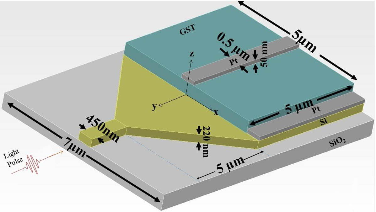
    Figure 1.Proposed design for the impulse response analysis of the GST-based PD device.

    The boundary condition is set to the perfectly matched layer (PML) with a maximum layer of 64 to avoid any back scattering. The stability factor and sampling rate are set to 1 and 0.05fs along with the minimum meshing of 0.25 nm to balance the solution convergence and time taken. All the simulations are performed considering the material to be defect free in order to understand the mechanism easily. The optical properties of aGST and cGST are taken from Ref. [20], whereas the mobility and recombination time are taken from Refs. [21] and [22], respectively. Platinum (Pt) metal is used as the contacts. A short pulse source is applied through the waveguide, whose pulse length is kept less than 10 fs with an offset of 30 fs with the desired wavelength at a central peak. The contact width and spacing between the contacts (mid-to-mid) are kept at 0.5 μm and 2.75 μm, respectively. The mentioned electric field variation is kept so high to ensure the proper drift velocity for the EHP separation. Also, due to this high field variation, the potential distribution does not fluctuate with the short pulse response period. Figure 2(a) shows the potential distribution at the time of impulse exposure. Figure 2(b) is a snapshot of electric field distribution in the x−y plane of the device, taken at 1 ps time and y=2μm position.

    For the 150 nm thick cGST on 220 nm thick Si at the time of illumination: (a) potential distribution at 4 V, 2 V, and 0.5 V biasing, (b) electric field distribution for 2 V biasing.

    Figure 2.For the 150 nm thick cGST on 220 nm thick Si at the time of illumination: (a) potential distribution at 4 V, 2 V, and 0.5 V biasing, (b) electric field distribution for 2 V biasing.

    Total current (J0) is calculated for both stable phases of GST and different bias voltages, thicknesses, and operating wavelengths. The carrier current variation is also calculated to understand the overall nature of the device. Figure 3 presents the impulse response of the modeled device. As the GST is a p-type material and the mobility of the hole is much higher than that of the electron, a very short current in the negative direction can be observed. This is due to the early arrival of the hole at the cathode, which is compensated by the displacement current (Jd) at the anode. This negative current remains for a very short time of 0.01ps. The displacement current (Jd) is immediately compensated by the hole current. Afterward, the response drastically increases as the level of optical illumination increases. Despite the higher hole mobility, due to the lower electric field at the cathode [Fig. 2(b)], the collection of holes is slower at the time of illumination. As a result, the holes are residing for a long time, even after 50 ps, and hence, a long tail can be observed. Still, an ultrafast response with FWHM 1ps is found in the investigations. The BW can be obtained by taking the Fourier transform of the impulse response curve, which yields the band width of 28GHz (3dB) at the 1550 nm wavelength source for the 150 nm thick cGST biased at 2 V.

    Carrier current (Jc), displacement current (Jd), and total current (J0) for a 150 nm thick cGST biased at 2 V illuminated at 1550 nm. The current component’s behavior is shown in the inset.

    Figure 3.Carrier current (Jc), displacement current (Jd), and total current (J0) for a 150 nm thick cGST biased at 2 V illuminated at 1550 nm. The current component’s behavior is shown in the inset.

    As the impulse response depends upon the dimensions, bias, and illumination condition, different simulations have been carried out by changing these parameters. Figure 4 illustrates the thickness dependence on the impulse response. It can be observed that as the thickness increases, the current becomes slightly lower, resulting in low responsivity for higher thicknesses with an exception at 210 nm. The inset in Fig. 4 shows the behavior of responsivity of both phases of GST at different thicknesses. However, the FWHM increases for higher thicknesses, resulting in the 3 dB BW of 28 GHz for 150 nm, whereas it is 43 GHz for the 210 nm thick cGST.

    J0 for different thicknesses of cGST biased at 2 V for 1550 nm wavelength illumination with the responsivity of both phases of GST at different thicknesses under similar illumination and biasing conditions. The variation in responsivity with thickness at 1550 nm is shown in the inset.

    Figure 4.J0 for different thicknesses of cGST biased at 2 V for 1550 nm wavelength illumination with the responsivity of both phases of GST at different thicknesses under similar illumination and biasing conditions. The variation in responsivity with thickness at 1550 nm is shown in the inset.

    A comparison between aGST and cGST in terms of total current (J0) is presented in Fig. 5. A large current difference can be observed for a short pulse excitation of the device for a very short duration. Though the aGST has the higher mobility, the much lower absorption coefficient puts a limit on the peak current and, hence, limits the magnitude for the 3 dB BW.

    Total current (J0) for the 150 nm thick aGST and cGST biased at 2 V illuminated at 1550 nm.

    Figure 5.Total current (J0) for the 150 nm thick aGST and cGST biased at 2 V illuminated at 1550 nm.

    A very important parameter for the communication application point of view is how the device is behaving at different wavelengths. Along with FWHM and responsivity, the BW can estimate the suitable application and viability of the device. If the BW changes its range by changing the material phase without any significant change in magnitude (responsivity), the device can be tuned for broadband applications. The impulse response of the cGST- and aGST-based PDs is shown in Figs. 6(a) and 6(b), respectively, illuminated by 1150 nm, 1550 nm, and 1850 nm wavelength light sources for the 150 nm thick GST biased at 2 V. The cGST is providing the highest current at the 1550 nm wavelength with the highest FWHM of 0.8ps, whilst at the 1150 nm wavelength, it shows the highest tail in the current. Excitation at 1850 nm shows a very low current with respect to other wavelengths. The aGST-based PD shows a very interesting behavior, as the responses have a broad second peak, which might be due to the sufficient collection of holes after some time. Initially, the collection is prevented due to its low dielectric constant, which results in the non-uniform distribution of the electric field.

    Impulse response of device illuminated at wavelengths of 1150 nm, 1550 nm, and 1850 nm for a 2 V biased 150 nm thick (a) cGST and (b) aGST.

    Figure 6.Impulse response of device illuminated at wavelengths of 1150 nm, 1550 nm, and 1850 nm for a 2 V biased 150 nm thick (a) cGST and (b) aGST.

    Also, in aGST, the 1150 nm wavelength excitation has the highest magnitude of current with the lowest at 1550 nm with an almost equal FWHM of 0.6ps (with the first peak). The approximate calculated values of the responsivity and BW are summarized in Table 1 for a 150 nm thick GST biased at 2 V. It can be observed from Table 1 that cGST is providing a better figure of merit with good BWs and responsivity, while aGST is also comparable in performances. The proposed device can be tuned for a broad range of spectrum by tuning the material phases.

    Responsivity (A/W)BW (GHz)
    Wavelength (nm)aGSTcGSTaGSTcGST
    115022575
    155018.521829
    18501841.5

    Table 1. Responsivity and Bandwidth Comparison of aGST and cGST

    In conclusion, a chalcogenide material (GST)-based silicon-on-insulator (SOI) waveguide-integrated PD is simulated for impulse response analysis. The two stable phases of GST, i.e., aGST and cGST, are used as the sensing element. Impulse response for the total current as well as the carrier current is addressed by solving the drift-diffusion model using FDTD. The device is illuminated with a very short pulse of a pulse width of 10 fs at different wavelengths. The behavior of the device studied in terms of current and an ultrafast response in both phases with an FWHM value less than 1 ps is observed. A sharp fall can be observed, which varies according to the thickness variation and illuminating wavelength and deciding the BW. aGST shows an interesting behavior with a second broad peak in its response. The aGST and cGST device performances are compared in terms of the total current obtained by varying the thickness and application wavelengths. For the viability of the PD, we have calculated the BW and responsivity and compared both phases at different wavelengths of the NIR range. It is found that cGST has the highest BW of 75 GHz at 1150 nm of illuminating wavelength with 25A/W responsivity for 150 nm thick layer biased at 2 V. However, aGST possesses a quite lower BW of 8 GHz with 18.5A/W responsivity at optical-fiber communication wavelength of 1550 nm with the same thickness and biasing. However, the cGST is still better than aGST at the 1550 nm wavelength. A broad range of spectrum in the NIR can be detected using the single material by tuning its phases, which may pave a new way for investigations.

    References

    [1] S. Raoux, F. Xiong, M. Wuttig, E. Pop. MRS Bull., 39, 703(2014).

    [2] D. Trommer, G. Unterbörsch, D. Schumann, O. Reimann, D. Huhse, D. Bimberg. Optical Fiber Communication Conference, WF7(2003).

    [3] A. E. Willner, S. Khaleghi, M. R. Chitgarha, O. F. Yilmaz. J. Light. Technol., 32, 660(2014).

    [4] K. Meyer, M. Pessot, G. Mourou, R. Grondin, S. Chamoun. Appl. Phys. Lett., 53, 2254(1988).

    [5] G. M. Dunn, A. B. Walker, A. J. Vickers, V. R. Wicks. J. Appl. Phys., 79, 7329(1996).

    [6] D. Kuhl, F. Hieronymi, E. H. Bottcher, D. Bimberg, J. Kuhl, M. Klingenstein. J. Light. Technol., 10, 753(1992).

    [7] S. E. J. Mahabadi, C. R. Menyuk. Frontiers in Optics(2017).

    [8] M. Wuttig, H. Bhaskaran, T. Taubner. Nat. Photon., 11, 8(2017).

    [9] T. A. Miller, M. Rudé, V. Pruneri, S. Wall. Phys. Rev. B, 94, 024301(2016).

    [10] L. Waldecker, T. A. Miller, M. Rudé, R. Bertoni, J. Osmond, V. Pruneri, R. E. Simpson, R. Ernstorfer, S. Wall. Nat. Mater., 14, 991(2015).

    [11] H. Liang, R. Soref, J. Mu, A. Majumdar, X. Li, W. P. Huang. J. Light. Technol., 33, 1805(2015).

    [12] Y. Huang, Y. Shen, C. Min, G. Veronis. Opt. Mat. Express, 8, 1672(2018).

    [13] W. Zheng, T. Xie, Y. Zhou, Y. L. Chen, W. Jiang, S. Zhao, J. Xu, Y. Jing, Y. Wu, G. Chen, Y. Guo, J. Yin, S. Huang, H. Q. Xu, Z. Liu, H. Peng. Nat. Commun., 6, 6972(2015).

    [14] V. Srivastava, M. Tolani, Sunny, R. Kumar. IEEE Sens. J., 18, 540(2018).

    [15] V. Srivastava, M. Tolani, Sunny. Superlatt. Microsctruct., 130, 1(2019).

    [16] J. Yin, Z. Tan, H. Hong, J. Wu, H. Yuan, Y. Liu, C. Chen, C. Tan, F. Yao, T. Li, Y. Chen, Z. Liu, K. Liu, H. Peng. Nat. Commun., 9, 3311(2018).

    [17] S. L. Chuang. Physics of Photonic Devices(2009).

    [18] B. G. Streetman, S. Banerjee. Solid State Electronic Devices(2009).

    [19] K. S. Yee. IEEE Trans. Antennas Propaga., 14, 302(1966).

    [20] J. Orava, T. Wágner, J. Šik, J. Přikryl, M. Frumar, L. Beneš. J. Appl. Phys., 104, 043523(2008).

    [21] A. Pirovano, A. L. Lacaita, A. Benvenuti, F. Pellizzer, R. Bez. IEEE Trans. Electron. Devices, 51, 452(2004).

    [22] A. V. Kolobov, J. Tominaga. Chalcogenides, 164, 3(2012).

    Vibhu Srivastava, Prateek Mishra, Sunny. Impulse response of Ge2Sb2Te5-based ultrafast photodetector integrated with SOI waveguide[J]. Chinese Optics Letters, 2019, 17(10): 100401
    Download Citation